| Issue |
EPJ Photovolt.
Volume 16, 2025
Special Issue on ‘EU PVSEC 2024: State of the Art and Developments in Photovoltaics’, edited by Robert Kenny and Gabriele Eder
|
|
|---|---|---|
| Article Number | 8 | |
| Number of page(s) | 7 | |
| DOI | https://doi.org/10.1051/epjpv/2024051 | |
| Published online | 15 January 2025 | |
https://doi.org/10.1051/epjpv/2024051
Original Article
24% Efficient TOPCon-based back contacted polyZEBRA solar cells
International Solar Energy Research Center Konstanz e.V., Rudolf-Diesel-Str. 15, 78467 Konstanz, Germany
* e-mail: This email address is being protected from spambots. You need JavaScript enabled to view it.
Received:
16
July
2024
Accepted:
3
December
2024
Published online: 15 January 2025
Abstract
This publication serves as an update on the progress of the back contacted polyZEBRA solar cell technology, which features Tunnel Oxide Passivating Contact (TOPCon) structures on both polarities. The solar cell efficiency mean values published by the end of last year have been improved by +1%abs to 24.0%. Following the key parameter changes, it is discussed how this improvement has been achieved. These changes are in particular the cell thickness and base resistivity, a dedicated wet-chemical cleaning step, the rear AlOx capping layer thickness and the pitch of the rear metallization pattern.
Key words: polyZEBRA / back contact / IBC / TOPCon / poly-Si
© J. Linke et al., Published by EDP Sciences, 2025
 This is an Open Access article distributed under the terms of the Creative Commons Attribution License (https://creativecommons.org/licenses/by/4.0), which permits unrestricted use, distribution, and reproduction in any medium, provided the original work is properly cited.
1 Introduction
Industrial solar cell mass production currently undergoes the transition from the Passivated Emitter and Rear Cell (PERC) to the Tunnel Oxide Passivating Contact (TOPCon) technology [1]. Even though impressive improvements of the achieved solar cell conversion efficiencies have been reported in the last months [2], this technology will eventually be limited by the classically diffused front side. This limitation may be overcome by applying poly-Si/SiOx TOPCon structures not only on the n-polarity, but also on the p-polarity. Due to the strong parasitic absorption of poly-Si layers [3,4], on the front side it has to be structured below the metal fingers [5–9]. Even more efficient is the application of both polarities poly-Si/SiOx contacts on the rear side of the solar cell with a poly-Si free front side with no parasitic absorption at all. Such back contacted cell concepts were addressed in scientific literature already several years ago [10,11]. However, these concepts were not further developed towards industrial application, probably due to the applied high-cost photolithography technique for rear side patterning. Instead, it was decided to omit the TOPCon structure on the p-polarity and make use of a PERC-like local aluminum back surface field in the so-called POLO-IBC hybrid cell design [12]. In contrast, IBC cells featuring TOPCon structures on both polarities have already been established in the industry by Maxeon Solar Technologies (SunPower) and Aiko Solar. The challenge of back contacted solar cells is to reach cost-competitiveness to standard both side contacted solar cells, considering the complex requirements of the rear side patterning. Within the TOPCon-based back contacted polyZEBRA solar cell concept developed at ISC Konstanz [13] this challenge is tackled by using only industrially established low-cost equipment, i.e. laser patterning and screen-printing, in order to yield comparable $/kWh costs as standard both side contacted TOPCon technology.
In a previous publication from last year [14] a mean solar cell efficiency of ∼23% was reported for the polyZEBRA cell concept along with simulations suggesting a roadmap to higher efficiencies. The present study serves as an update of the development progress and reports a recent mean value of 24.0% solar cell efficiency, which is +1%abs compared to last year's publication. It is analyzed how this improvement has been achieved. In particular, the influence of the cell thickness and base resistivity, a dedicated wet-chemical cleaning step, the rear AlOx capping layer thickness and the pitch of the rear metallization pattern is addressed.
2 Material and methods
For this study, polyZEBRA solar cells were fabricated according to the process flow shown in Figure 1, which is the same process flow used for fabrication of the solar cells discussed in last year's publication [14] and in all experiments in between. The base material were Cz-grown n-type wafers in M6 format with a thickness of 150 μm. On the rear side, the emitter and base regions feature poly-Si/SiOx contacts and are separated by a p-type diffused gap region. The interfacial tunnel oxides were thermally grown (∼2 nm) and capped with low-pressure chemical vapor deposited (LPCVD) (n) poly-Si (Fig. 1, step 2) and (i) poly-Si (Fig. 1, step 6), respectively. A first BBr3-diffusion was applied for the background p-type doping of the initially undoped (i) poly-Si and the resulting boron silicate glass (BSG) was removed in hydrofluoric acid (HF) (Fig. 1, step 7). The thermal budget (965 °C) of the second BBr3-diffusion for p-type doping of the gap and front side region also activates the passivation of the poly-Si/SiOx structures on both polarities (Fig. 1, step 10). Details regarding the laser-based patterning steps (Fig. 1, step 4, 8) can be found in [15,16]. Plasma-enhanced chemical vapor deposited (PECVD) stacks of AlOx capped with a SiNx layer were used for passivation of the surfaces. The metal contacts were screen-printed with Ag-containing paste for both fingers and busbars (BB) and a pitch of the rear metallization pattern of 800 μm and 6BB.
Alongside with the cells, all experiments include reference wafers which follow the exact same process, but the laser patterning of the rear side creates 40 × 40 mm2 squares of the individual cell regions (n poly-Si/SiOx, p poly-Si/SiOx, gap/front side) instead of the narrow straight line pattern for the cells. These squares enable characterization methods, which would not be applicable to the lines as thin as 500 μm. In order to separate the effect of single parameter changes, results of further experiments are shown, in which a specific parameter change was explicitly tested against a dedicated control group.
In last year's publication, different cappings of the rear AlOx passivation were tested, namely “Capping A” as control group and “Capping B” with improved capping. The group with improved capping showed higher cell efficiencies, but nevertheless, all results of the present study are compared to the control group of last year's publication. The reason is that the improved capping showed much worse passivation quality on cell precursors before metallization, an issue that could not be fixed until now. In this sense, all improvements of the present study are benchmarked against this control group of [14].
Table 1 shows the differences in experimental parameters between last year's control group and the cells from the present study. The final cell thickness is a bit thinner due to thinner as-delivered wafers and optimizations of the alkaline etching steps throughout the process. One outcome of last year's study supported to use wafers with a lower base resistivity as the loss in current was overcompensated by a gain in fill factor. Thus, also a lower base resistivity was chosen for the present study. Another difference is the omitting of a dedicated cleaning after alkaline texturing in addition to the standard cleaning. In order to reduce last year's strong recombination below the metal-semiconductor interfaces, the thickness of the rear AlOx capping has been increased with the goal to minimize spiking of the metal through the interfacial oxide of the poly-Si/SiOx structure. In addition, the pitch of the rear side metallization pattern was reduced, which increases the density of fingers and thus increases the charge carrier collection efficiency. It should be noted that the thermal budget and interfacial oxide thicknesses, whose tuning is of high relevance for poly-Si/SiOx structures, has not been altered since last year's publication and was the same in all experiments presented in this contribution.
The IV curves of the solar cells were recorded using a conventional Halm flasher. The individual regions of the cells were characterized by quasi steady-state photoconductance (QSSPC) measurements with a Sinton Lifetime Tester on the reference wafers featuring the squares as described above. Additionally, some cells were excluded as precursors before metallization in order to enable QSSPC measurements on the actual IBC pattern.
The experimental data is supported by simulations done with Quokka3 [17]. The most important input parameters are based on measurement data of test structures, which reflect the process flow and parameters used for the fabrication of the solar cells (Fig. 1). They are listed in Table 2. The bulk lifetime (τbulk) was adjusted in order to match the simulated open-circuit voltage (Voc) to the experimentally determined implied open-circuit voltage (iVoc) with the metal recombination turned off. Subsequently, the metal recombination of the (n) poly-Si/SiOx was fixed to 50 fA/cm2 while the metal recombination of the (p) poly-Si/SiOx was adjusted in order to match the simulated Voc to the experimentally determined Voc.
Most important simulation input parameters based on measurement data of test structures, which represent the process flow and parameters used for the fabrication of the solar cells.
3 Results and discussion
Figure 2 shows the IV data of the solar cells and iVoc values of the cell precursors before metallization of last year's publication and of the present study. First of all it is evident, that the scattering of the fill factor (FF) data from last year's publication is much larger. This is attributed to contacting problems with the IV measurement chuck, which have been solved in the meantime.
All cell parameters show significant improvement apart from the short circuit current density Jsc. The differences in the mean values are +1.8%abs in cell efficiency, −0.2 mA/cm2 in Jsc, +10 mV in iVoc, +17mV in Voc, +4.3%abs in pFF and +4.7%abs in FF. Furthermore, the iVoc-to-Voc loss, which serves as a measure for the total recombination at the metal-semiconductor interfaces, was decreased by −7 mV and the pFF-to-FF loss, which serves as a measure for the series resistance Rser, was reduced by −0.4%abs. In the following it is discussed, how the changes in experimental parameters as summarized in Table 1 can explain these differences in the cells' IV data.
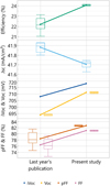 |
Fig. 2 Solar cell parameters determined by IV measurements of the polyZEBRA cells from last year's publication [14] and the present study. The iVoc values were taken from QSSPC measurements on cell precursors before metallization. |
3.1 Wafer thickness and base resistivity
The wafers of last year's publication and the present study were provided by different suppliers with different characteristics. The wafers used in the present study were thinner as-delivered with 150 μm compared to 175 μm before. Furthermore, the base resistivity was lower with ∼4 Ωcm compared to ∼13 Ωcm, a choice which was taken based on the lower series resistance that is expected from lower resistivity wafers in [14,18]. From simulations the thinner wafer would cause a loss in Jsc of ∼0.03 mA/cm2 and the lower base resistivity a loss of ∼0.18 mA/cm2, which in sum is able to explain the experimentally observed loss of ∼0.2 mA/cm2.
A lower base resistivity also implies a lower series resistance, which is experimentally accessible via the smaller pFF-to-FF loss, as shown in Figure 3. It has reduced from ∼2%abs to ∼1.6%abs, which corresponds to a relative reduction of 20%. However, from the simulation the series resistance is reduced by only 2.5%, so other effects seem to be contributing to the lower series resistance as will be discussed in the upcoming sections.
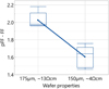 |
Fig. 3 pFF-to-FF loss as a measure for the cell's series resistance Rser as function of wafer thickness and resistivity from last year's publication [14] (175 μm, ∼13 Ωcm) and the present study (150 μm, ∼4 Ωcm). |
3.2 Dedicated cleaning after texture
Due to historical reasons from the development of the process sequence a dedicated cleaning process after alkaline texture was used in addition to the standard pSC1 (KOH/H2O2) and HF/HCl clean. In this additional step, the wafers were rinsed in HF/HCl once again, dipped for 10 min into piranha solution (H2SO4/H2O2 mixture) at elevated temperature and the resulting oxide was stripped in HF. Since such additional cleaning is uncommon, especially from an industrial point of view, it was tested to skip it. The cells without additional cleaning showed a ∼3 mV higher Voc compared to the control group, which was also confirmed by the iVoc of cell precursors before metallization. QSSPC measurements on the reference wafers featuring squares of the individual regions revealed, that this improvement in iVoc occurs only on the (p) poly-Si/SiOx regions while the (n) poly-Si/SiOx and the gap/front side regions are unaffected. We speculate that the (p) poly-Si layers has some pinholes through which the etch solution could reach and damage the buried interfacial oxide. If so, all wet chemical steps should be kept to a minimum duration and thus skipping the additional cleaning showed a beneficial effect.
3.3 Rear AlOx capping thickness
The rear side of a back contacted cell is commonly covered by a large metal fraction as well as by a large fraction of heavily light absorbing poly-Si layers [3,4]. Hence, bifaciality plays a minor role and so the capping of the rear AlOx does not necessarily have to be optimized towards optimum light trapping. On the other hand, the properties of the capping significantly influence the metallization, as also discussed in [14,19,20]. In particular, the thickness is expected to influence both the recombination current density at the metal-semiconductor interfaces J0,met as well as the series resistance Rser. Figure 4 shows the iVoc-to-Voc loss as measure for J0,met and the pFF-to-FF loss as measure for Rser for the capping thickness applied in last year's publication and for a ∼15 nm thicker capping.
The iVoc-to-Voc loss decreases by ∼3 mV for the thicker mask, meaning that the J0,met is reduced. A similar decreasing J0,met for thicker dielectric stack was reported before [20]. As the firing conditions were the same, this phenomenon is explained by a larger amount of SiNx capping to be etched by the paste, which reduces the total area of metal inside the poly-Si layer. And this in turn implies a lower area of damaged or penetrated interfacial oxide, eventually reducing the J0,met and increasing the Voc.
Based on this reasoning, an increase in Rser is expected from the higher contact resistance from the lower amount of metal in the poly-Si layer. This increase in Rser is reflected in the ∼0.2%abs higher mean and median pFF-to-FF loss values for the thicker capping (Fig. 4), though the scattering is large. It is expected however, that the gain in Voc will overcompensate the slightly higher Rser. Unfortunately, it was not possible to validate this hypothesis with the achieved cell efficiencies, as the group with thicker capping showed a much lower Jsc than the control group, which is not a consequence of the thicker capping as confirmed by a follow-up experiment.
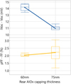 |
Fig. 4 iVoc-to-Voc loss as a measure for the recombination at the metal-semiconductor interfaces J0,met and pFF-to-FF loss as a measure for the cell's series resistance Rser for a rear AlOx capping thickness of 60 nm in last year's publication [13] and a follow-up experiment with ∼15 nm thicker capping. |
3.4 Pitch of rear metallization pattern
The pitch of the rear metallization pattern determines the total number of fingers on the cell. This in turn influences the charge carrier collection [18], the total recombination current at the metal-semiconductor interfaces and the light reflection on the rear side and as such the bifaciality. In order to boost the charge carrier collection and decrease the series resistance, the pitch was reduced from 1080 μm in last year's publication to 800 μm without changing the finger dimensions. The corresponding changes in the emitter, base and gap widths are listed in Table 3. The effects on the iVoc-to-Voc loss and the pFF-to-FF loss are shown in Figure 5.
On the one hand, the pFF-to-FF loss as a measure for Rser is significantly reduced with the smaller pitch to less than 50% of the value of the control group. Due to the smaller distance between two fingers of the same polarity, the charge carriers need to travel a shorter distance until they are collected by the fingers and so the series resistance reduces. This effect is mostly responsible for the reduction of pFF-to-FF loss between last year's publication and the present study as presented in Figure 3.
On the other hand, the larger number of fingers causes a larger total area of metal-semiconductor interfaces from spiking through the interfacial oxide and in turn a higher total recombination current in the whole cell. This effect materializes for the smaller pitch in +4 mV of the iVoc-to-Voc loss as a measure for the total recombination current.
Nevertheless, as the solar cell efficiency is ∼0.4%abs higher for the pitch of 800 μm, the gain in Rser overcompensated the loss in J0,met.
Differences in emitter, base and gap widths under reduction of the pitch of the rear metallization.
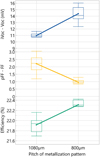 |
Fig. 5 iVoc-to-Voc loss as a measure for the recombination at the metal-semiconductor interfaces J0,met, pFF-to-FF loss as a measure for the cell's series resistance Rser and solar cell efficiency from an intermediate experiment comparing the pitch of the rear metallization pattern of 1080 μm as used in last year's publication [14] to a smaller pitch of 800 μm as used in the present study. |
3.5 Remaining parameter gains
The above described explicit changes in process parameters can explain the gain in cell efficiency only partly. For instance, the iVoc of the cell precursors before metallization has improved by +10 mV, even though the dedicated cleaning after texture did only yield +3 mV. Also, the iVoc-to-Voc loss was reduced by 7 mV from 14 to 7 mV, but the decrease caused by the thicker rear AlOx capping (Fig. 4) and the increase caused by the lowered pitch of the rear metallization pattern (Fig. 5) just cancel each other out. Since last year's publication and the present study 14 cell batches with 100 wafers each have been processed. As nearly the entire wafer handling was done manually, such a large number of batches leads to a learning curve of the operators. Also, minor changes to individual process parameters without explicit tests against a control group probably also have improved the iVoc Another potential contribution is an improved wafer quality from recent deliveries.
Another beneficial effect could have been the change towards a four times larger laser spot from 30 × 30 μm2 to 30 × 130 μm2 rectangular top-hat geometry. Laser top-hat spot edges typically provide less fluence to the substrate than the homogenous bulk of the spot, an issue that was addressed by a certain overlap of neighboring spots. For the larger spot the area fraction of these overlapping regions is lower because of the lower edge-to-bulk ratio. Assuming a locally worse passivation in these overlapped regions, the reduced area fraction of the overlapping regions of the larger spot could have increased the iVoc.
But also the other way round, the strong reduction in pFF-to-FF loss by more than 50% from the smaller pitch (Fig. 5) suggests a much larger reduction than has been observed between last year's publication and the present study (Fig. 3). However, the large scattering of the data of the control group weakens the meaningfulness of the 50% reduction, which is based on a comparison of the mean values. Simulations with the smaller pitch support this interpretation with a predicted Rser reduction of ∼30%, which is closer to the 20% reduction experimentally observed between last year's publication and the present study.
4 Conclusion and outlook
The polyZEBRA solar cell efficiency mean value of 23.0% from last year's publication was improved by 1%abs. to 24.0%. The major changes of the process parameters were analyzed, but are not consistently able to explain all the parameter gains. The remaining improvements are attributed to a general learning curve of the manual processing steps and minor parameter adjustments without explicit control groups. Next steps to further boost the cell efficiency are the minimization of the iVoc-to-Voc loss while maintaining the high FF by an improved metallization sequence and the general increase of the passivation of the individual regions of the cell, i.e. the minimization of the recombination J0,pass on the front side, in order to increase the Voc.
Acknowledgments
The authors would like to thank all colleagues at ISC Konstanz that have contributed indirectly in the laboratory and administration as an essential part of the research process and functionality of the institute.
Funding
This work was supported by the project “IBC4EU” and has received funding from the European Union's Horizon Europe research and innovation programme under grant agreement No. 101084259.
Conflicts of interest
The authors have nothing to disclose.
Data availability statement
Reported data can be provided upon request.
Author contribution statement
Conceptualization: J.Li., C.P. and F.B.; Methodology: J.Li., C.P. and F.B.; Validation, J.Li., C.P., J.H., S.S.K., V.M. and F.B.; Formal Analysis: J.Li. and C.P.; Investigation: J.Li., C.P. and S.S.K.; Resources: F.B.; Data Curation: J.Li., C.P. and F.B.; Writing − Original Draft Preparation: J.Li.; Writing − Review & Editing: J.Li., C.P., J.H., S.S.K., V.M., J.Lo. and F.B.; Supervision: J.Lo. and F.B.; Project Administration: F.B.; Funding Acquisition: F.B. All authors have read and agreed to the published version of the manuscript.
References
- M. Fischer, M. Woodhouse, P. Baliozian, International Technology Roadmap for Photovoltaics (ITRPV) 2023 Results, VDMA Photovoltaics Equipment, 15th Edition (2024). https://www.vdma.org/international-technology-roadmap-photovoltaic [Google Scholar]
- A. Mette, S. Hörnlein, F. Stenzel, R. Hönig, I. Höger, M. Schaper, K. Petter, M. Junghänel, C. Klenke, A. Weihrauch, H.-C. Ploigt, O. Kwon, A. Schönmann, O. Tobail, K. Kim, A. Schwabedissen, M. Kauert, K. Duncker, B. Faulwetter-Quandt, J. Scharf, J. Cieslak, F. Kersten, B. Lee, S. T. Kristensen, O. Schnelting, C. Baer, M. Queck, G. Zimmermann, L. Burtone, L. Niebergall, M. Schütze, S. Schulz, M. Fischer, S. Peters, F. Fertig, J. W. Müller, Q. ANTUM NEO with LECO Exceeding 25.5% cell Efficiency, Sol. Energy Mater. Sol. Cells 277, 113110 (2024). https://doi.org/10.1016/j.solmat.2024.113110 [Google Scholar]
- J. Steffens, Dependencies between poly-Si composition and solar cell performance of poly-Si/SiOx passivating contacts, Ph.D. thesis, Universität Konstanz, Konstanz, Germany, 2020. http://nbn-resolving.de/urn:nbn:de:bsz:352-2-19tzla6vns71f7 [Google Scholar]
- F. Feldmann, M. Nicolai, R. Müller, C. Reichel, M. Hermle, Optical and electrical characterization of poly-Si/SiOx contacts and their implications on solar cell design, Energy Procedia, 124, 31 (2017). https://doi.org/10.1016/j.egypro.2017.09.336 [CrossRef] [Google Scholar]
- J. Hoß, S.S. Kalaghichi, M. Comak, P. Preis, J. Lossen, J. Linke, L. Koduvelikulathu, F. Buchholz, Advanced TOPCon solar cells with vanishing metal induced recombination losses, EPJ Photovolt. 15, 43 (2024). https://doi.org/10.1051/epjpv/2024040 [Google Scholar]
- S.-P. Hsu, C.-P. Huang, K.-C. (Jay)Lai, C.-C. Li, B.-C. Kung, S.-Y. Chen, M.-T. Kuo, H.-C. Chang, Localized bifacial passivated contacts solar cell with 23.5% efficiency, in Proc. of 40th European Photovoltaic Solar Energy Conference and Exhibition EUPVSEC (Lisbon, 2023), p. 020042. https://doi.org/10.4229/EUPVSEC2023/1CV.3.1 [Google Scholar]
- F. Meyer, A. Ingenito, J. J. Diaz Leon, X. Niquille, C. Allebé, S. Nicolay, F.-J. Haug, C. Ballif, Localisation of front side passivating contacts for direct metallisation of high-efficiency c-Si solar cells, Sol. Energy Mater. Sol. Cells 235, 111455 (2022). https://doi.org/10.1016/j.solmat.2021.111455 [CrossRef] [Google Scholar]
- J. Wang, S.P. Phang, T.N. Truong, Z. Li, H.T. Nguyen, D. Macdonald, J. Stuckelberger, Inkjet-printed boron-doped poly-Si/SiOx passivating contacts, Sol. Energy Mater. Sol. Cells 272, 112928 (2024). https://doi.org/10.1016/j.solmat.2024.112928 [CrossRef] [Google Scholar]
- B. Uygun, S. Kluska, J.-I. Polzin, J. Schube, M. Jahn, K. Krieg, R. Turan, H. Nasser, Local p+ Poly-Si passivating contacts realized by direct FlexTrail printing of boron ink and selective alkaline etching for high efficiency TOPCon based solar cells, Authorea (2024). https://doi.org/10.22541/au.172114744.47084956/v1 [Google Scholar]
- F. Haase, C. Hollemann, S. Schäfer, A. Merkle, M. Rienäcker, J. Krügener, R. Brendel, R. Peibst, Laser contact openings for local poly-Si-metal contacts enabling 26.1%-efficient POLO-IBC solar cells, Sol. Energy Mater. Sol. Cells, 186, 184 (2018). https://doi.org/10.1016/j.solmat.2018.06.020 [CrossRef] [Google Scholar]
- G. Yang, P. Guo, P. Procel, G. Limodio, A. Weeber, O. Isabella, M. Zeman, High-efficiency black IBC c-Si solar cells with poly-Si as carrier-selective passivating contacts, Sol. Energy Mater. Sol. Cells, 186, 913 (2018). https://doi.org/10.1016/j.solmat.2018.06.019 [CrossRef] [Google Scholar]
- F. Haase, C. Hollemann, S. Schafer, J. Krugener, R. Brendel, R. Peibst, Transferring the record p-type Si POLO-IBC cell technology towards an industrial level, in IEEE 46th Photovoltaic Specialists Conference (PVSC) (Chicago, IL, USA, 2019), p. 2200. https://doi.org/10.1109/PVSC40753.2019.8980960 [Google Scholar]
- J. Linke, F. Buchholz, V. Mihailetchi, C. Peter, J. Hoß, J. Lossen, R. Kopecek, Fully passivating contact IBC solar cells using laser processing, in Proc. of 8th World Conference on Photovoltaic Energy Conversion WCPEC (Milan, Italy, 2022), p. 102. https://doi.org/10.4229/WCPEC-82022-1CV.2.11 [Google Scholar]
- J. Linke, F. Buchholz, S. Sharbaf, J. Hoß, V. Mihailetchi, J. Lossen, R. Kopecek, Progress in development of polyZEBRA IBC solar cells, in Proc. of 40th European Photovoltaic Solar Energy Conference and Exhibition EUPVSEC (Lisbon, Portugal, 2023) p. 020046. https://doi.org/10.4229/EUPVSEC2023/1CV.3.3 [Google Scholar]
- F. Buchholz, J. Linke, J. Hoss, H. Chu, V. Mihailetchi, A. Chaudhary, J. Lossen, R. Kopecek, E. Wefringhaus, Local passivating contacts from laser doped p+ polysilicon, in Proc. of 38th European Photovoltaic Solar Energy Conference and Exhibition EUPVSEC (Online, 2021), p. 140. https://doi.org/10.4229/EUPVSEC20212021-2BO.11.3 [Google Scholar]
- S. Sharbaf Kalaghichi, J. Hoß, R. Zapf-Gottwick, J.H. Werner, Laser activation for highly boron-doped passivated contacts, Solar 3, 362 (2023). https://doi.org/10.3390/solar3030021 [CrossRef] [Google Scholar]
- A. Fell, Quokka3, v2.4.6. (2024), www.quokka3.com [Google Scholar]
- K.R. McIntosh, M.J. Cudzinovic, D.D. Smith, W.P. Mulligan, R.M. Swanson, The choice of silicon wafer for the production of low-cost rear-contact solar cells, in Proc. of 3rd World Conference on Photovoltaic Energy Conversion WCPEC (Osaka, Japan, 2003), p. 971 [Google Scholar]
- J. Linke, F. Buchholz, C. Peter, J. Hoß, J. Lossen, R. Kopecek, The role of masking layers during metallization of poly-Si/SiOx contacts, in Proc. of Silicon PV 2022 (Konstanz, Germany, 2023), p. 02004. https://doi.org/10.1063/5.0141842 [Google Scholar]
- V.D. Mihailetchi, H. Chu, R. Kopecek, Insight into metal induced recombination losses and contact resistance in industrial silicon solar cells, in Proc. of 7th World Conference on Photovoltaic Energy Conversion WCPEC (Waikoloa Village, HI, 2018), p. 2673. https://doi.org/10.1109/PVSC.2018.8547888 [Google Scholar]
Cite this article as: Jonathan Linke, Christoph Peter, Jan Hoß, Saman Sharbaf Kalaghichi, Valentin Mihailetchi, Jan Lossen, Florian Buchholz, 24% Efficient TOPCon-based back contacted polyZEBRA solar cells, EPJ Photovoltaics 16, 8 (2025)
All Tables
Most important simulation input parameters based on measurement data of test structures, which represent the process flow and parameters used for the fabrication of the solar cells.
Differences in emitter, base and gap widths under reduction of the pitch of the rear metallization.
All Figures
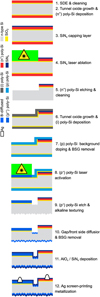 |
Fig. 1 PolyZEBRA solar cell fabrication process flow based on [13]. |
| In the text | |
|
Fig. 2 Solar cell parameters determined by IV measurements of the polyZEBRA cells from last year's publication [14] and the present study. The iVoc values were taken from QSSPC measurements on cell precursors before metallization. |
| In the text | |
|
Fig. 3 pFF-to-FF loss as a measure for the cell's series resistance Rser as function of wafer thickness and resistivity from last year's publication [14] (175 μm, ∼13 Ωcm) and the present study (150 μm, ∼4 Ωcm). |
| In the text | |
|
Fig. 4 iVoc-to-Voc loss as a measure for the recombination at the metal-semiconductor interfaces J0,met and pFF-to-FF loss as a measure for the cell's series resistance Rser for a rear AlOx capping thickness of 60 nm in last year's publication [13] and a follow-up experiment with ∼15 nm thicker capping. |
| In the text | |
|
Fig. 5 iVoc-to-Voc loss as a measure for the recombination at the metal-semiconductor interfaces J0,met, pFF-to-FF loss as a measure for the cell's series resistance Rser and solar cell efficiency from an intermediate experiment comparing the pitch of the rear metallization pattern of 1080 μm as used in last year's publication [14] to a smaller pitch of 800 μm as used in the present study. |
| In the text | |
Current usage metrics show cumulative count of Article Views (full-text article views including HTML views, PDF and ePub downloads, according to the available data) and Abstracts Views on Vision4Press platform.
Data correspond to usage on the plateform after 2015. The current usage metrics is available 48-96 hours after online publication and is updated daily on week days.
Initial download of the metrics may take a while.