| Issue |
EPJ Photovolt.
Volume 17, 2026
Special Issue on ‘EU PVSEC 2025: State of the Art and Developments in Photovoltaics', edited by Robert Kenny and Carlos del Cañizo
|
|
|---|---|---|
| Article Number | 12 | |
| Number of page(s) | 9 | |
| DOI | https://doi.org/10.1051/epjpv/2026005 | |
| Published online | 10 March 2026 | |
https://doi.org/10.1051/epjpv/2026005
Original Article
Electro-thermal energy yield simulations for bifacial all-perovskite tandem modules
1
Fluxim AG, Katharina-Sulzer-Platz 2, 8400 Winterthur, Switzerland
2
Fraunhofer Institute for Solar Energy Systems ISE, Heidenhofstr. 2, 79110 Freiburg, Germany
3
TNO partner of Solliance, High Tech Campus 21, Eindhoven, 5656 AE, The Netherlands
4
Zurich University of Applied Sciences ZHAW, Technikumstrasse 71, 8400 Winterthur, Switzerland
* e-mail: This email address is being protected from spambots. You need JavaScript enabled to view it.
Received:
12
October
2025
Accepted:
29
January
2026
Published online: 10 March 2026
Abstract
The energy yield of bifacial all-perovskite tandem modules is quantified for a selected outdoor testing location using electro-thermal simulations on cell and module levels combined with a model providing spectral irradiance according to geographical location and time. Cell level modelling is performed using an opto-electronic drift-diffusion-Poisson simulation on the full tandem device under consideration of direct and diffuse front illumination according to the sun position and atmosphere model, and diffuse rear illumination according to the ground albedo. On module level we combine a two-dimensional finite-element large area simulation of the electrodes in an optimized layout for a 100 cm2 monolithically interconnected module with the one-dimensional active area coupling law obtained from the simulated cell level characteristics. Thereby, thermal effects are considered regarding heat generation by light absorption, charge carrier transport and recombination, as well as heat transport through the stack and dissipation at the surface. To reduce the computational cost, operation conditions are binned with respect to limiting photocurrent, ambient temperature, and wind speed. After verification of the validity of the binning approach by comparison with full time-data modelling, it is used to compute the annual energy yield on cell level as a function of ground albedo and top cell band gap, confirming both, a large gain from bifaciality already at moderate albedo and the benefit from lower band gap top cells for high rear irradiation level due to large ground reflectivity. Finally, thermal effects and configuration-dependent cell-to-module losses are quantified via the evaluation of annual energy yield with the full electro-thermal module simulation, using the binned cell-level characteristics as well as the measured ambient temperature and wind speed as input. The results imply that an accurate assessment of upscaling losses is more critical for a reliable quantification of energy yield than consideration of the full temperature dependence.
Key words: All-perovskite tandems / multi-scale simulation / energy yield / bifacial / electro-thermal / thin-film modules
© U. Aeberhard et al., Published by EDP Sciences, 2026
 This is an Open Access article distributed under the terms of the Creative Commons Attribution License (https://creativecommons.org/licenses/by/4.0), which permits unrestricted use, distribution, and reproduction in any medium, provided the original work is properly cited.
1 Introduction
All-perovskite tandem (APT) photovoltaics is promising as a scalable and flexible, yet high-efficiency all-thin film solar power conversion technology [1]. In two-terminal configuration, due to spectral sensitivity, the device architecture benefits from optimization according to the local spectral irradiance conditions, for which annual energy yield (EY) rather than the power conversion efficiency (PCE) under standard test conditions (STC) needs to be evaluated. Using advanced modelling of spectral irradiance in combination with compact electrical models for APT, it was shown that depending on the local ground reflectivity – encoded in the albedo value – bifacial architectures can be beneficial regarding EY [2]. Furthermore, bifaciality alters the ideal band gap combination in the tandem architecture, with lower top cell band gaps being favored due to the larger photogeneration in the bottom cell [3–10]. In the case of APT, where band gaps can be tuned in a wide range of values, this is of particular significance as it proved to be challenging to achieve both, efficient and stable wide band gap perovskites. The second deviation from STC performance in the evaluation of EY regards the variation in operating temperature – obtained from thermal models under consideration of heating due to light absorption and cooling from heat dissipation at the module surface - which affects significantly the operation of the solar cells due to the prevalence of thermally activated processes [11,12].
Here, we aim at quantifying the impact of details in cell- and module level design and architecture on the site-specific annual EY of bifacial APT modules as developed in the SuPerTandem project [13]. We therefore need an approach that goes beyond compact cell-level models [2,14,15] – which are restricted to global electrical device characteristics in terms of terminal currents - or an electro-thermal circuit model for single junction perovskite modules [11], but is rather similar in spirit to the comprehensive modelling frameworks discussed in [16,17] for perovskite-silicon tandem modules, albeit for an all-thin-film technology implemented using monolithic interconnection.
The paper is organized as follows. In Section 2, we outline such a multi-scale electro-thermal simulation approach capable of propagating configurational details to module-level EY performance variation. The prediction of the model for STC performance of bifacial APT solar cells and for the annual EY at a specific location on cell and module level are given in Section 3, followed by concluding remarks in Section 4.
2 Material and methods
The multi-scale simulation approach adopted for this work is represented schematically in Figure 1. The procedure starts with the computation of the direct and diffuse components of the solar spectral irradiance in time intervals of 30 min for the location of the outdoor testing facility at Fraunhofer ISE in Freiburg, Germany. For the evaluation of the angles of incidence, the actual orientation of the module as shown in Figure 3 is used, which is south-facing (azimuth of 180°) with a tilt angle of 32°. The spectra are obtained from an implementation of the SMARTS model from NREL [18] together with a sun position algorithm available in the device simulation tool SETFOS [19]. Serving as input for the optical simulation with SETFOS based on the transfer matrix method (TMM) including coherent thin films and incoherent thick layers, the spectra are used to compute the limiting sub-cell photocurrent as well as the charge photogeneration profile inside the APT device stack from TNO (Fig. 2), using the parametrization obtained in [20]. Thereby, the contributions of direct and diffuse components from frontside illumination are added to the rear-side contribution from diffuse ground reflection, for which a Lambertian distribution is assumed and the total incident spectrum is scaled by the albedo value. To reduce the computational cost, binning of operating conditions [14,16] is performed with respect to limiting photocurrent - obtained from the inexpensive optical simulation as a function of the spectral irradiance condition - as well as ambient temperature Tamb and wind speed (WS), for which measured data from the outdoor testing location as provided by Fraunhofer ISE is used (Fig. 3). The average irradiance is well captured by the simulation with SETFOS. The binning for one year with 30 min time intervals (total count of 17520 instances) is shown in Figure 4 for the isothermal case (binning wrt photocurrent only), the case without wind cooling (binning wrt photocurrent and Tamb), and the full data (binning wrt photocurrent, Tamb and WS). Full (isothermal) opto-electronic device simulation based on the drift-diffusion-Poisson framework including mobile ions and explicit models for charge transfer at the recombination junction [21] is then performed with SETFOS for the operating conditions representative of the individual bins. The energy level diagram of the electrical model with parameters based again on a previous calibration for a very similar device [20] (see SI of this reference for a discussion of the parameter extraction) is shown in Figure 2b. Figure 5a shows a selection of the direct and diffuse spectra for a photocurrent binning with 32 bins (displayed are bins No. 1,2,3,7,13,32), where the binning is performed wrt the average of the limiting photocurrent (corresponding to a resolution of 0.5 mA/cm2). As compared to binning wrt irradiance, such a binning is more representative of device operation as it captures photocurrent mismatch issues originating from spectral changes as apparent in the spectra (e.g. pronounced red-shift at low-light conditions due to predominance of large angles of incidence). The binning approach is validated by comparing the binned EY for the opaque APT cell from TNO to the EY as obtained from the simulation with the full time data, i.e., evaluating the contribution of each 30 min interval for a single month. As can be inferred from Figure 5b, there is a fast convergence to a value deviating by less than 1% from the full simulation result. In the following, EY is therefore evaluated with 32 photocurrent bins.
The temperature-dependent current-voltage characteristics (JVT curves) resulting from the opto-electronic simulation are then fed together with the bin-specific absorbed optical power to the electro-thermal module simulation as implemented in the large area semiconductor simulation tool LAOSS [22]. The “2D+1D” simulation approach solves Ohm’s law and the heat equation in the 2D electrode layers via the finite element method. The electrodes are connected vertically by the JVT law that acts as a local source term. In this way, the impact of spatial non-uniformities and local effects such as shunts or point defects can be captured and the suitability of realistic module layouts regarding cell dimension and laser scribes for monolithic interconnection can be assessed [20]. Also here, the module parametrization obtained in [20] is used. On the other hand, the thermal model – coupled to the electrical simulation via the JVT curves – reflects heating of the module due to light absorption, recombination, and Joule heating (inferred from the JVT coupling law), as well as heat transport through the stack and dissipation/cooling at the surface [23]. The connection to the wind speed is established via the standard expression of heat transfer with a constant and a wind-speed dependent term [24].
Finally, the module simulation for binned operating conditions provides the binned module power, from which the annual EY can be inferred via multiplication with the bin counts and the data acquisition time interval.
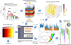 |
Fig. 1 Schematic representation of the workflow for the multi-scale energy yield simulation of bifacial all-perovskite tandem solar modules: Generation of irradiation spectra, optical simulation, binning wrt limiting photocurrent and ambient temperature, electrical device simulation (binned), electro-thermal module simulation (binned). |
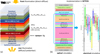 |
Fig. 2 (a) Composition and layout of the bifacial APT device stack from TNO simulated in this work. In the opaque variant, the 180 nm ITO contact layer is replaced by a silver layer of the same thickness. (b) Implementation of the device stack for optical and electrical simulation with the 1D device simulation tool SETFOS. |
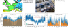 |
Fig. 3 Outdoor testing location and installation at Fraunhofer ISE in Freiburg (Germany) and corresponding measurements of operating conditions regarding global irradiance, ambient temperature, and wind speed. Shown are data for one year (1.6.2023-31.5.2024). The orange wind speed data is the half-hourly average of the full data with higher time resolution. |
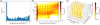 |
Fig. 4 Binning wrt operating conditions: (a) limiting photocurrent (isothermal case, 25 °C), (b) limiting photocurrent and ambient temperature, (c) limiting photocurrent, Tamb and wind speed. |
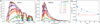 |
Fig. 5 Spectral irradiance corresponding to the average limiting photocurrent per bin: (a) Direct and diffuse component. Shown are the spectra for bins No. 1, 2, 3, 7, 13, and 32 (binning wrt. maximum limiting photocurrent). (b) Convergence of the EY for the opaque reference module wrt. number of photocurrent bins (reference is simulation with full time data for one month). |
3 Results
3.1 Performance of bifacial APT under standard test conditions
Simulations are performed for the device stack from TNO (Fig. 2a) with a wide band gap (WBG) perovskite top-cell absorber with Egtop = 1.5–1.8 eV and a narrow band gap (NBG) perovskite bottom cell absorber with Egbot = 1.25 eV. The refractive index data used is based primarily on the information provided in the SI of reference [25] and is given in Figure S1 of the Supporting Information. Figure 6a shows the active layer absorptance of an APT solar cell with Egtop = 1.77 eV in presence and absence of a back mirror, which illustrates the transmission losses for front illumination at long wavelengths in the bifacial case. Figure 6b then displays the corresponding photogeneration profile under STC and for the different configurations of the rear contact: opaque (Ag mirror), bifacial (ITO back contact) without rear illumination, and bifacial with rear illumination corresponding to a diffuse (Lambertian) reflection with an albedo of 0.3 (rear irradiance of 300 W/m2).
As shown in Table 1, which provides the sub-cell photocurrents at the optical limit, the opaque and the bifacial device without rear illumination are bottom limited, whereas for a rear irradiance of Irear = 300 W/m2, the gain due to rear illumination outweighs significantly the transmission loss due to the absence of an opaque mirror and pushes the device to top-limitation in the bifacial case. The current-voltage (JV) characteristics of the electrical simulation calibrated with measured data from TNO for a bifacial architecture without rear illumination are displayed in Figure 6c. Moving to an opaque rear reflector increases the current and reduces the current mismatch, but lowers also the fill-factor, whereas rear illumination improves both performance parameters. The large amount of excess current in the bottom cell under rear illumination is reflected in the high level of recombination current (dashed lines) at low voltages. The same picture is found at the radiative limit, where non-radiative recombination is turned off (Fig. 6d). The impact of cell temperature on the cell JV characteristics is shown in Figures 6e and 6f, again for the fitted model and its radiative limit, respectively. At the radiative limit, the two dominant features observed are the reduction of fill factor (FF) at low temperatures due to the lower efficiency of thermally activated transport processes – e.g. across interface barriers – and the decrease of open circuit voltage (VOC) at large temperatures due to growing strength of thermally activated recombination processes. In the presence of non-radiative recombination via bulk and interface defects, the temperature dependence of the recombination dominates.
Variation of sub-cell band gaps result in redistribution of photocurrent generation due to front and rear illumination. As larger tandem photocurrents are targeted, and adjusting the top cell band gap is both feasible and attractive from a stability perspective, the investigation is restricted to this modification at fixed bottom-cell band gap. Full optimization would require adjustment of both band gaps and absorber thicknesses, which is straightforward to achieve using the present approach, but is beyond the scope of this work. The dependence of the power output on rear irradiance and top-cell band gap under STC is displayed in Figure 7. In (a), the evaluation is performed for the fitted model that includes non-radiative recombination. To obtain an upper limit of performance for the selected device configuration, recombination losses are limited to the radiative channel in (b). In both cases, a clear benefit from lower top-cell band gaps at larger levels of rear-side contribution is apparent.
In Figure 8, the current-voltage characteristics resulting from an electro-thermal module simulation under maximum front irradiance and albedo of 0.3 are plotted for the radiative limit and as a function of ambient temperature for the 10 × 10 cm2 monolithically interconnected bifacial APT module with 31 cell stripes and geometric fill factor GFF≈0.91 (see Ref. [20] for configurational details). In (a) the situation is shown without heating activated, while heating from absorption and transport is present in (b). The temperature dependence of the cell level characteristics (Fig. 6f) results not only in the expected reduction of VOC at elevated temperatures, but also in FF losses at low temperatures due to thermal activation of transport, which underlines the relevance of the advanced device model used. Under these conditions and for the parametrization of the thermal model chosen, the absorption of solar irradiation leads to a positive difference between junction and ambient temperatures of around 15 °C–25 °C, in agreement with values found in the literature [11]. The largest heating effect is thereby found for the lowest WS values at short circuit and at large voltages beyond Voc, while heating is least pronounced at MPP. The cell/module temperature as a function of ambient temperature at short circuit, open circuit, and MPP is shown in the Supporting Information (Fig. S2a) together with the translation of the PCE vs ambient temperature to PCE vs module temperature (Fig. S2b).
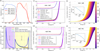 |
Fig. 6 (a) Active layer (front) absorptance for opaque and bifacial all-perovskite tandem solar cell devices. (b) Photogeneration rate profile of the all-perovskite tandem solar cell for opaque, semi-transparent and bifacial architectures (AM1.5g spectrum), normal incidence, rear irradiance of 300 W/m2). (c,d) Current-voltage characteristics of the bifacial APT device from TNO used for model calibration (no rear illumination), as well as the corresponding projection to opaque and bifacial (with rear illumination) variants, with non-radiative recombination and at the radiative limit. (e,f) Temperature dependence of the isothermal current-voltage characteristics for the semitransparent device under AM1.5g illumination as obtained from electro-thermal simulation using the fitted model and its radiative limit. |
Optical sub-cell currents generated under normal incidence and AM1.5g front illumination and diffuse rear illumination at moderate albedo of 0.3 for opaque and semitransparent architectures. *denotes limiting sub-cell.
 |
Fig. 7 Photovoltaic output power for AM1.5g normal front illumination and diffuse rear illumination, as a function of top-cell band gap and rear illumination intensity, for (a) the fitted model and (b) the radiative limit. |
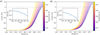 |
Fig. 8 Module current-voltage characteristics as a function of ambient temperature: (a) Case without heating, (b) with heating due to absorption and transport (no recombination heating at the radiative limit). The insets show the variation of PCE with ambient temperature. |
3.2 Quantification of energy yield on cell and module levels
Figure 9a displays the relative change of annual energy yield for a bifacial APT at the radiative limit as compared to the opaque reference, as a function of ground reflectance and for two different values of the top-cell absorber band gap. While already small values of albedo favor the bifacial over the opaque architecture, the benefits are massively increased for lower Egtop – which is in part due larger current mismatch in the opaque cell - and do not saturate quickly with increasing rear-side contribution. The impact of the level of detail in electrical and thermal simulation – i.e., the qualitative and quantitative effect of simplifying assumptions on the energy harvesting - is demonstrated in Figures 9b and 9c for the case of the 1.6 eV band gap top cell with optimized bifacial EY, at the radiative limit and including non-radiative losses, respectively. Consideration of the actual variation in ambient temperature results in a small increase in cell-level EY as compared to simulations at constant temperature of 25 °C, which can be explained by the lower average temperatures on the test site (as seen in Fig. 3). On the same level of thermal effects, i.e., under consideration of variation in ambient temperature but no heating, the step to electrical module simulation induces a significant EY reduction related to opto-electronic cell-to-module losses (dead area, TCO resistivity). It needs to be emphasized that this does not include losses from deteriorated active area quality (as often found when using large-area coating processes), as using the small-area characteristics for the coupling law amounts to the assumption of preserved absorber quality. Consideration of the internal heat generation due to light absorption and Joule heating reduces the annual EY further. Inclusion of wind cooling, on the other hand, results in only a small recovery of EY. While there is a drop of close to 35% in EY from the radiative limit to the case with non-radiative losses, this decrease is much lower than the 50% drop of STC power generation inferred from Figure 7. The qualitative picture is very similar in the two cases, however, the relative cell-to-module losses in EY are less pronounced in the presence of non-radiative recombination, but thermal losses on module level are more severe. Inspection of bifacial gain (at an albedo of 0.3 and Egtop = 1.6 eV) finally shows a decrease from over 60% on cell level at the radiative limit to below 50% on module level with non-radiative losses losses (cf Fig. S3 in the Supporting Information that includes the opaque reference), which is in part due to the larger resistivity of the transparent back electrode in the bifacial configuration as compared to the opaque module with full silver rear mirror.
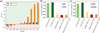 |
Fig. 9 Impact of bifaciality on EY for cell and module levels: (a) Bifacial gain at the radiative limit as a function of albedo for two different values of top cell band gap, revealing the vast increase and slower saturation of the benefits from bifaciality at reduced band gap. (b,c) Annual EY for the 1.6 eV band gap top cell, on cell level at fixed temperature, with temperature variation but no heating, module level EY at ambient temperature, module level with heating and under consideration of wind cooling, for the radiative limit and including non-radiative losses, respectively. |
4 Conclusion and future directions
Access to full opto-electronic cell-level and electro-thermal module-level simulations enables the quantification of the relative gain and losses in EY related to bifaciality, temperature, and module layout details. Optimization of the top cell band gap results in significant increase of EY that is largely maintained when up-scaling from cells to thin-film modules, and holds also in the presence of non-radiative losses.
The present approach, while living up to existing comprehensive state-of-the-art modelling frameworks for photovoltaic EY quantification, may still be refined in several aspects. On the one hand, the use of meteorological data can be extended to include a cloud cover model similar to the approach in [2,15]. Clouds reduce the direct radiation and increase the diffuse component, which would shift energy harvesting from normal incidence to more shallow angles. Hence, their impact can be easily accommodated in the present approach.
On the other hand, the temperature dependence of intrinsic material parameters such as, e.g., the optical constants should also be considered, as they can impact the sub-cell photocurrent magnitude and thereby the current matching. This, however, requires the availability of suitable experimental data for calibration. While non-radiative losses have been considered in the quantification of energy yield, a detailed analysis of the different sub-cell specific loss channels and their impact on EY is also enabled by the present approach. Last but not least, the quantitative comparison with measured outdoor performance data will require an extension of the framework to include models for device degradation as linked to operating conditions [26].
Acknowledgments
This work has benefited from stimulating discussions with Sandra Jenatsch and Davide Moia from Fluxim, as well as from the exchange within the SuPerTandem project consortium.
Funding
This work received funding from the European Union's Horizon Europe research and innovation programme under grant agreement No 101075605, project SuPerTandem, and through the Swiss State Secretariat for Education, Research and Innovation (SERI) under grant no. 22.00379/101075605.
Conflicts of interest
UA, AS, RHA, RHI, BB, and BR are employed by Fluxim AG that commercializes the software tools SETFOS and LAOSS used in this work.
Data availability statement
Data associated with this article can be obtained from the corresponding author upon reasonable request.
Author contribution statement
Conceptualization, U.A.; Methodology, U.A.; Software, A.S., R.H.A., R.H.I., B.B.; Validation, U.A., R.H.A.; Formal Analysis, U.A.; Investigation, U.A.; Resources, B.R., S.V., M.K.; Data Curation, U.A., M.K., M.N.; Writing – Original Draft Preparation, U.A.; Writing – Review & Editing, U.A.; Visualization, U.A.; Project Administration, U.A., M.K., S.V.; Funding Acquisition, B.R., S.V., M.K.
Supplementary Material
Optical material parameters used in the simulation (spectral nk-data), thermal data (module heating), full data of EY vs model (including opaque reference).
Figure S1. Refractive indices (n, black) and extinction coefficients (k, red) of the materials used in the optical simulation of the all-perovskite tandem solar cell from TNO.
Figure S2. (a) Temperature of the cell vs ambient temperature under maximum irradiance and at different points of operation of the device. (b) Power conversion efficiency as a function of cell temperature.
Figure S3. Full annual energy yield data at (a) the radiative limit and (b) with non-radiative losses, for a bifacial module with a top-cell absorber band gap of 1.6 eV and assuming an albedo value of 0.3. The dotted line marks the value for the opaque reference (with Ag back contact).
Access Supplementary MaterialReferences
- P. Wu, D.T. Gangadharan, M.I. Saidaminov, H. Tan, A roadmap for efficient and stable all-perovskite tandem solar cells from a chemistry perspective, ACS Cent. Sci. 9, 14 (2023). https://doi.org/10.1021/acscentsci.2c01077 [Google Scholar]
- F. Gota, S.X. An, H. Hu, B. Abdollahi Nejand, U.W. Paetzold, Energy yield modeling of bifacial all-perovskite two-terminal tandem photovoltaics, Adv. Optical Mater. 11, 2201691 (2023). https://doi.org/10.1002/adom.202201691 [Google Scholar]
- Y. Blom, M.R. Vogt, O. Isabella, R. Santbergen, Optimization of the perovskite cell in a bifacial two-terminal perovskite/silicon tandem module, Sol. Energy Mater. Sol. Cells 282, 113431 (2025). https://doi.org/10.1016/j.solmat.2025.113431 [Google Scholar]
- A. Onno et al., Predicted power output of silicon-based bifacial tandem photovoltaic systems, Joule 4, 580 (2020). https://doi.org/10.1016/j.joule.2019.12.017 [CrossRef] [Google Scholar]
- M.T. Patel, R. Asadpour, J. Bin Jahangir, M. Ryyan Khan, M.A. Alam, Current-matching erases the anticipated performance gain of next-generation two-terminal Perovskite-Si tandem solar farms, Appl. Energy 329, 120175 (2023). https://doi.org/10.1016/j.apenergy.2022.120175 [Google Scholar]
- H. Hao et al., Energy yield prediction of bifacial perovskite/silicon tandem photovoltaic modules, Sol. RRL 7, 2300218 (2023). https://doi.org/10.1002/solr.202300218 [Google Scholar]
- L. Xu, F. Xu, J. Liu, X. Zhang, A.S. Subbiah, S. De Wolf, Bandgap optimization for bifacial tandem solar cells, ACS Energy Lett. 8, 3114 (2023). https://doi.org/10.1021/acsenergylett.3c01014 [Google Scholar]
- M. De Bastiani et al., Efficient bifacial monolithic perovskite/silicon tandem solar cells via bandgap engineering, Nat. Energy 6, 167 (2021). https://doi.org/10.1038/s41560-020-00756-8 [Google Scholar]
- K. Jäger, P. Tillmann, E.A. Katz, C. Becker, Perovskite/silicon tandem solar cells: effect of luminescent coupling and bifaciality, Sol. RRL 5, 1 (2021). https://doi.org/10.1002/solr.202000628 [Google Scholar]
- J. Lehr et al., Energy yield of bifacial textured perovskite/silicon tandem photovoltaic modules, Sol. Energy Mater. Sol. Cells 208, 110367 (2020). https://doi.org/10.1016/j.solmat.2019.110367 [Google Scholar]
- P. Lopez-Varo, M. Amara, S. Cacovich, A. Julien, A. Yaïche, M. Jouhari, J. Rousset, P. Schulz, J.-F. Guillemoles, J.-B. Puel, Dynamic temperature effects in perovskite solar cells and energy yield, Sust. Energy Fuels 5, 5523 (2021). https://doi.org/10.1039/D1SE01381E [Google Scholar]
- M.R. Vogt et al., Developing an energy rating for bifacial photovoltaic modules, Prog. Photovolt. Res. Appl. 31, 1466 (2023). https://doi.org/10.1002/pip.3678 [Google Scholar]
- Super Tandem. https://supertandem.eu [Google Scholar]
- O. Dupré, A. Tuomiranta, Q. Jeangros, M. Boccard, P.-J. Alet, C. Ballif, Design rules to fully benefit from bifaciality in two-terminal perovskite/silicon tandem solar cells, IEEE J. Photovolt. 10, 714 (2020). https://doi.org/10.1109/JPHOTOV.2020.2973453 [Google Scholar]
- R. Schmager, M. Langenhorst, J. Lehr, U. Lemmer, B.S. Richards, U.W. Paetzold, Methodology of energy yield modelling of perovskite-based multi-junction photovoltaics, Optics Express 27, A507 (2019). https://doi.org/10.1364/OE.27.00A507 [Google Scholar]
- M.R. Vogt, C. Ruiz Tobon, A. Alcañiz, P. Procel, Y. Blom, A. Nour El Din, T. Stark, Z. Wang, E. Garcia Goma, J.G. Etxebarria, H. Ziar, M. Zeman, R. Santbergen, O. Isabella, Introducing a comprehensive physics-based modelling framework for tandem and other PV systems, Sol. Energy Mater. Sol. Cells 247, 111944 (2022). https://doi.org/10.1016/j.solmat.2022.111944 [Google Scholar]
- P. Procel, Y. Zhou, M. Verkou, M. Leonardi, D. Di Girolamo, G. Giuliano, O. Dupré, Y. Blom, M.R. Vogt, R. Santbergen, F. Rametta, M. Foti, C. Gerardi, M. Zeman, O. Isabella, PV multiscale modelling of perovskite / silicon two-terminal devices: from accurate cell performance simulation to energy yield prediction, Sol. Energy Mater. Sol. Cells 293, 113864 (2025). https://doi.org/10.1016/j.solmat.2025.113864 [Google Scholar]
- C. Gueymard, SMARTS2, A simple model of the atmospheric radiative transfer of sunshine: algorithms and performance assessment, Rep. FSEC-PF-270-95, Florida Solar Energy Center (1995). http://www.fsec.ucf.edu/en/publications/pdf/FSEC-PF-270-95.pdf [Google Scholar]
- Setfos v5.5 by Fluxim AG. www.fluxim.com/setfos [Google Scholar]
- U. Aeberhard, N. Natsch, A. Schneider, S.J. Zeder, H. Carrillo-Nuñez, B. Blülle, B. Ruhstaller, Multi-scale simulation of reverse-bias breakdown in all-perovskite tandem photovoltaic modules under partial shading conditions, Sol. RRL 8, 2400492 (2024). https://doi.org/10.1002/solr.202400492 [Google Scholar]
- U. Aeberhard, S. Zeder, B. Ruhstaller, Effects of photon recycling and luminescent coupling in all‐perovskite tandem solar cells assessed by full opto‐electronic simulation, Sol. RRL 8, 2400264 (2024). https://doi.org/10.1002/solr.202400264 [Google Scholar]
- Laoss v4.2 by Fluxim AG. www.fluxim.com/laoss [Google Scholar]
- M. Diethelm, L. Penninck, M. Regnat, T. Offermans, B. Zimmermann, C. Kirsch, R. Hiestand, S. Altazin, B. Ruhstaller, Finite element modeling for analysis of electroluminescence and infrared images of thin-film solar cells, Sol. Energy 209, 186 (2020). https://doi.org/10.1016/j.solener.2020.08.058 [Google Scholar]
- D. Faiman, Assessing the outdoor operating temperature of photovoltaic modules, Prog. Photovolt.: Res. Appl. 16, 307 (2008). https://doi.org/10.1002/pip.813 [CrossRef] [Google Scholar]
- K. Datta et al., Monolithic all‐perovskite tandem solar cells with minimized optical and energetic losses, Adv. Mater. 34, 2110053 (2022). https://doi.org/10.1002/adma.202110053 [Google Scholar]
- S. Orooji, U.W. Paetzold, Energy yield modeling of perovskite–silicon tandem photovoltaics: degradation and total lifetime energy yield, Energy Technol. 12, 2400998 (2024). https://doi.org/10.1002/ente.202400998 [Google Scholar]
Cite this article as: Urs Aeberhard, Andreas Schiller, Roger Häusermann, Roman Hiestand, Balthasar Blülle, Markus Kohlstädt, Mehrdad Najafi, Sjoerd Veenstra, Beat Ruhstaller, Electro-Thermal Energy Yield Simulations for Bifacial All-Perovskite Tandem Modules, EPJ Photovoltaics 17, 12 (2026), https://doi.org/10.1051/epjpv/2026005
All Tables
Optical sub-cell currents generated under normal incidence and AM1.5g front illumination and diffuse rear illumination at moderate albedo of 0.3 for opaque and semitransparent architectures. *denotes limiting sub-cell.
All Figures
|
Fig. 1 Schematic representation of the workflow for the multi-scale energy yield simulation of bifacial all-perovskite tandem solar modules: Generation of irradiation spectra, optical simulation, binning wrt limiting photocurrent and ambient temperature, electrical device simulation (binned), electro-thermal module simulation (binned). |
| In the text | |
|
Fig. 2 (a) Composition and layout of the bifacial APT device stack from TNO simulated in this work. In the opaque variant, the 180 nm ITO contact layer is replaced by a silver layer of the same thickness. (b) Implementation of the device stack for optical and electrical simulation with the 1D device simulation tool SETFOS. |
| In the text | |
|
Fig. 3 Outdoor testing location and installation at Fraunhofer ISE in Freiburg (Germany) and corresponding measurements of operating conditions regarding global irradiance, ambient temperature, and wind speed. Shown are data for one year (1.6.2023-31.5.2024). The orange wind speed data is the half-hourly average of the full data with higher time resolution. |
| In the text | |
|
Fig. 4 Binning wrt operating conditions: (a) limiting photocurrent (isothermal case, 25 °C), (b) limiting photocurrent and ambient temperature, (c) limiting photocurrent, Tamb and wind speed. |
| In the text | |
|
Fig. 5 Spectral irradiance corresponding to the average limiting photocurrent per bin: (a) Direct and diffuse component. Shown are the spectra for bins No. 1, 2, 3, 7, 13, and 32 (binning wrt. maximum limiting photocurrent). (b) Convergence of the EY for the opaque reference module wrt. number of photocurrent bins (reference is simulation with full time data for one month). |
| In the text | |
|
Fig. 6 (a) Active layer (front) absorptance for opaque and bifacial all-perovskite tandem solar cell devices. (b) Photogeneration rate profile of the all-perovskite tandem solar cell for opaque, semi-transparent and bifacial architectures (AM1.5g spectrum), normal incidence, rear irradiance of 300 W/m2). (c,d) Current-voltage characteristics of the bifacial APT device from TNO used for model calibration (no rear illumination), as well as the corresponding projection to opaque and bifacial (with rear illumination) variants, with non-radiative recombination and at the radiative limit. (e,f) Temperature dependence of the isothermal current-voltage characteristics for the semitransparent device under AM1.5g illumination as obtained from electro-thermal simulation using the fitted model and its radiative limit. |
| In the text | |
|
Fig. 7 Photovoltaic output power for AM1.5g normal front illumination and diffuse rear illumination, as a function of top-cell band gap and rear illumination intensity, for (a) the fitted model and (b) the radiative limit. |
| In the text | |
|
Fig. 8 Module current-voltage characteristics as a function of ambient temperature: (a) Case without heating, (b) with heating due to absorption and transport (no recombination heating at the radiative limit). The insets show the variation of PCE with ambient temperature. |
| In the text | |
|
Fig. 9 Impact of bifaciality on EY for cell and module levels: (a) Bifacial gain at the radiative limit as a function of albedo for two different values of top cell band gap, revealing the vast increase and slower saturation of the benefits from bifaciality at reduced band gap. (b,c) Annual EY for the 1.6 eV band gap top cell, on cell level at fixed temperature, with temperature variation but no heating, module level EY at ambient temperature, module level with heating and under consideration of wind cooling, for the radiative limit and including non-radiative losses, respectively. |
| In the text | |
Current usage metrics show cumulative count of Article Views (full-text article views including HTML views, PDF and ePub downloads, according to the available data) and Abstracts Views on Vision4Press platform.
Data correspond to usage on the plateform after 2015. The current usage metrics is available 48-96 hours after online publication and is updated daily on week days.
Initial download of the metrics may take a while.