| Issue |
EPJ Photovolt.
Volume 16, 2025
|
|
|---|---|---|
| Article Number | 27 | |
| Number of page(s) | 12 | |
| DOI | https://doi.org/10.1051/epjpv/2025015 | |
| Published online | 03 June 2025 | |
https://doi.org/10.1051/epjpv/2025015
Original Article
Design, manufacture and characterization of compact optics for micro-CPV
1
Institut Interdisciplinaire d'Innovation Technologique (3iT), Université de Sherbrooke, 3000 Boulevard Université, Sherbrooke, J1K 0A5 Québec, Canada
2
Laboratoire Nanotechnologies Nanosystèmes (LN2) − CNRS IRL-3463, Institut Interdisciplinaire d’innovation Technologique, Université de Sherbrooke, 3000 Boulevard Université, Sherbrooke, J1K 0A5 Québec, Canada
3
Laboratoire Hubert Curien, Université de Lyon, UMR CNRS 5516, 42000 St Etienne, France
* e-mail: This email address is being protected from spambots. You need JavaScript enabled to view it.
Received:
14
February
2025
Accepted:
30
April
2025
Published online: 3 June 2025
Abstract
Concentrator photovoltaics (CPV) modules are complex, heavy and bulky which hinders the deployment of this technology. Over the past few years, the miniaturization of this technology, called micro-CPV, promises to make more compact and less expensive modules. This article focuses on the design, fabrication and characterization of a 350× single-stage concentrator optic made of PMMA. A matrix of 16 lenses has been produced, and a prototype module has been fabricated and characterized outdoors, achieving an optical efficiency of over 80%.
Key words: Optics / micro-CPV / III-V / multi-junctions solar cell
© C. Jouanneau et al., Published by EDP Sciences, 2025
 This is an Open Access article distributed under the terms of the Creative Commons Attribution License (https://creativecommons.org/licenses/by/4.0), which permits unrestricted use, distribution, and reproduction in any medium, provided the original work is properly cited.
1 Introduction
In recent years, solar energy has seen a drastic increase in production and a reduction in price, thanks to the large-scale production of silicon-based solar panels, which dominate the photovoltaic market. Silicon technologies are performing close to their theoretical limit, with a record of 27.6% for a silicon cell [1] and a theoretical limit of 29.43% [2]. To increase efficiency, a shift to new technologies is necessary. The solar cells currently achieving the highest conversion efficiencies are multi-junction cells based on III-V materials, with a record efficiency of 39.5% for triple junctions [1]. This technology produces more energy per unit area, which is necessary for new market where space is constrained (space solar, mobile solar charging systems, etc.) [3]. The major drawback of multi-junction cells is the price of III-V materials, typically two orders of magnitude more expensive than materials used on a large scale [4]. CPV technology reduces the cost of using III-V solar cells by concentrating light, minimizing the amount of III-V material needed. As well as saving costly III-V materials, concentrated light also boosts solar cell performance, resulting in an all-technology efficiency record of 47.6% for 4-junctions solar cell under 665× [1].
Still, CPV modules are complex (involving 1 [5], 2 [6] or 3 [7] stages of optics), heavy, and bulky. This increases their manufacturing costs, as well as the costs of installing and operating these solar panels on trackers that need to be robust enough to accommodate the weight of the modules [3]. In response to these limitations, a new CPV technology has emerged in recent years called micro-CPV. The idea behind this technology is to reduce the size of the solar cells to below 1 mm2, and consequently, the size and volume of the optics. Micro-CPV should thus allow the manufacture of more compact, lighter, and less expensive concentrator solar panels. A study conducted at NREL shows the strong competitive potential of micro-CPV compared to traditional CPV and silicon PV systems [8].
In the literature, micro-CPV modules using two optical stages exist, such as the Semprius module [9]. However, a study by Panasonic [10] demonstrates the relevance of using a single-stage optics approach for micro-CPV. Indeed, this study shows that the non-uniformity effects of light caused by using single-stage refractive optics are not problematic for submillimeter cells and, therefore, for micro-CPV technology.
Panasonic has published several articles presenting compact micro-CPV modules with a single optical stage made either entirely of polymethyl methacrylate (PMMA) [6,11,12], or of PMMA on a glass substrate [10,13]. However, these articles focus on the characterization of the modules and provide little information on the design, fabrication, and characterization of this type of optics. Our study will focus on the design, modeling, and characterization of a compact single stage optical system for micro-CPV made entirely of plastic PMMA.
First, the design of the optics for InGaP/InGaAs/Ge submillimetric solar cells has been carried out using the ZEMAX OpticStudio software (ray tracing) with different constraints defined at the beginning of the first section. The optics are then manufactured and characterized. In the last phase, a micro-CPV module prototype has been fabricated and measured outdoors. Then, a model of the optical losses has been compared to these results to determine the losses related to the optics for each sub-cell and for the entire cell.
2 Design and tolerancing of the optical system
In this section, concentrating optics are designed using ZEMAX optic studio ray tracing software. The aim is to produce a low-cost, lightweight and compact optic. Tolerances of the optics will also be studied to determine if the manufacturing uncertainties (such as alignment and optical design) remain acceptable for fabrication.
2.1 Definition of the criteria
The optics are made of plastic, more precisely PMMA, which is a standard low-cost material for plastic optics [14]. Moreover, PMMA optics are lightweight with good optical properties (transmittance above 90% at 500nm) [14].
Figure 1 shows a diagram of the optical system. To obtain a compact optic, the optical system is composed of a single optical stage and the maximum thickness of the optic made of PMMA is set at 2 cm, in line with publications on compact modules in the literature [6,10,11,13]. As shown in Figure 1, the lenses are square-shaped, allowing for a more compact lens array compared to round lenses and creating a square light spot that matches the shape of the solar cells.
IEC 62670 standard defined the acceptance angle as the angle at which more than 10% of the light is lost and set the minimum threshold at ±0.4°. With the focal length now set at around 2 cm, the geometric concentration is set at 350× for 0.25 mm2 cells so as to obtain a f-number (focal length divided by the diameter of the entrance pupil) between 1.5 and 2, which enables good optical efficiency (more than 80%) and an acceptance angle greater than 0.4° [14]. The concentration being set at 350× for 0.25 mm2 cells, each lens therefore has a surface area of 9.35× 9.35 mm2.
Since the optical system consists of a single stage refractive optics, it is prone to chromatic aberrations. Therefore, the lenses used are likely to cause a spread of the focal spot depending on the wavelength, which could lead to variations in the carrier generation regions between the different sub-cells. This type of aberration is not a problem if we optimise the uniformity of the light on the top cell to avoid resistive losses in the top cell's emitter layer [10]. To establish a criterion for light uniformity on the top cell, the peak to average ratio (PAR) is used. This value represents the maximum effective concentration (CPeak) on the cell divided by the average concentration across the cell surface (CMean) as shown in Equation (1).
 (1)
(1)
A lower PAR ratio corresponds to more uniform illumination. However, there's a trade-off between uniformity and the acceptance angle. Highly uniform illumination means the light spot covers the entire active area at normal incidence. When the angle of incidence increases, the spot undergoes a lateral shift. When it reaches the edge of the cell, any further shift causes part of the light to fall outside the cell, reducing the collected power and therefore narrowing the acceptance angle. In contrast, less uniform illumination (higher PAR), where the light spot is smaller than the cell, leaves an unilluminated margin and the edges of the cell. This margin accommodates spot movement under varying incidence angles, allowing light collection over a wider range of angles and thus increasing the acceptance angle. An upper bound for the PAR can be estimated through a first order approximation of the resistive and the shadowing losses. A maximum 10% power loss can then be imposed as an upper bound which then defines a condition on the PAR at 11.5 (details in Appendix A.2).
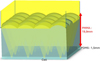 |
Fig. 1 Optical system diagram. The PMMA lenses are 19.9 mm-thick from the top of lenses. |
2.2 Design of the optical system
The first step in lens design is to consider spherical aberration. The effect of this aberration is that rays passing along the edge of the lens do not focus on the same point as rays passing through the center. As a result, the size of the image spot will be enlarged, which may lead to a drop in optical efficiency. Spherical aberrations can be cancelled out by modifying the conicity constant, which defines the deviation of the optical surface from a spherical shape. This factor is therefore set at −0.46 (the calculation of this value is available in Appendix A.1).
Figure 1 shows the optical system composed of a 19.9 mm thick PMMA lens, designed to meet the criterion of being less than 2 cm-thick, with a 1.5 mm layer of polydimethylsiloxane (PDMS) to attach the optics to the receiver.
With the thickness of the PMMA and PDMS and the value of the conicity constant now fixed, the curvature radius (Rc) was set to achieve a compromise between PAR (uniformity of the light) and acceptance angle. The Zemax simulation using Rc = 6.83 mm results in a PAR of 2.38 for the top cell which is below the PAR threshold of 11.5 needed to keep resistive losses below 10% power losses, and an acceptance angle of ±0.5° which is above the minimum threshold of ±0.4°. The chosen curvature radius therefore meets the PAR and acceptance angle criteria.
Figure 2 shows the effective concentration distribution on a 0.25 mm2 solar cell with the aforementioned Rc values, conicity constant, PMMA and PDMS thickness. Each image corresponds to a different wavelength, chosen to be the average absorption wavelength of each sub-cell: 500 nm for the top cell, 800 nm for the middle cell and 1300 nm for the bottom cell, from left to right respectively. On Figure 2, it can be seen that the uniformity of the light is optimised on the top cell. Moreover, the light spot is smaller for the middle and the bottom cell than for the top cell. It is important that the light spots for the middle and bottom cells are smaller than that for the top cell due to chromatic aberration; otherwise, we would lose light on the middle and bottom cells.
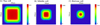 |
Fig. 2 ZEMAX optical simulation of the illuminance of a 0.25 mm2 solar cell as a function of wavelength A) 500 nm (top cell), B) 800 nm (middle cell) and C) 1300nm (bottom cell). The scale on the right of the images corresponds to the effective concentration. The average concentration is 350×, so from the maximum effective concentration of each sub-cell, we can calculate the PAR for each sub-cell: top cell: 2.38, middle cell: 6.85, bottom cell: 15.6. |
2.3 Tolerances
Now that the design is complete, we then varied the various parameters (Rc, conicity constant, PMMA and PDMS thickness) set previously, while keeping the others fixed, to estimate an approximation of the manufacturing tolerances for each of them. The tolerance is therefore not combined. In order to calculate the curvature radius tolerance, the minimum curvature radius (Rmin) is found when 10% of the light is lost (the image spot will grow as the radius of curvature decreases). The maximum curvature radius (Rmax) is found when the PAR reaches 11.5 (see Sect. 2.1). The curvature radius must necessarily be within the interval [Rmin, Rmax] to limit both light losses (<10%) and resistive losses (PAR < 11.5). To define a single tolerance value, we choose the most restrictive case, i.e. min(|Rc − Rmin|, |Rc − Rmax|) (Rc being the set values from the previous section). The same method is used to calculate tolerances for PMMA and PDMS thickness, and for the conicity constant. The misalignment tolerance is calculated when 10% of the light is lost (values are summarized in Tab. 1). This method allows for tolerance specification to a single digit but slightly narrows the tolerance range. Indeed, in the case of Rc, the limitation is set by Rmin (i.e min(|Rc − Rmin|, |Rc–Rmax|) = |Rc–Rmin|), enabling to achieve a curvature radius greater than +95 μm while still meeting the criteria. As curvature radius increases, PAR remains below 11.5 until Rc = 6.96 mm and there is no loss of light. Between Rc = 6.96 mm and Rc = 7.15 mm the PAR exceeds 11.5 and reach a maximum of 20, causing a maximum resistive losses of over 13% (see resistive model in Appendix A.2). Above Rc = 7.15 mm the PAR falls back below 11.5, but from Rc = 7.3 mm light losses of over 20% occur on the bottom cell (opposite situation to Fig. 2: the light spot is larger for the bottom cell wavelengths than for the top cell wavelengths). Since the bottom cell has excess current, curvature radius up to 7.3 mm allow the criteria to be met, except in the 6.96–7.15 mm range, where resistive losses up to 3% above the criteria may occur. The tolerances shown are given for information only, but they do have certain limitations. They are not combined and, as explained above (for Rc), it is possible to obtain values that differ from the tolerances and still meet our criteria. Table 1 summarizes the various design parameters and their tolerances.
Summary of the concentration optics parameters as well as its alignment tolerances and the specifications studied here.
 |
Fig. 3 Picture of a PMMA matrix lenses after molding. |
3 Optics characterization
Figure 3 shows a picture of a lens matrix at reception. To check the quality of the optics made by external service request, measurements were taken to check their thickness, curvature radius, conicity constant and optical losses.
For the thickness measurement, a digital caliper was used. Three different optical matrices were measured, the results are 19.90 ± 0.02 mm, 19.88 ± 0.02 mm and 19.86 ± 0.02 mm. The largest deviation measured in relation to the desired value is therefore 40 μm. The thickness tolerance calculated in the previous section was ±330 μm. The PMMA thickness complies with the design.
A confocal microscope was used to measure the curvature radius. A fit was then made using the equation for an aspheric lens (details of measurements and fits are given in the Appendix A.3). The measurements and fits were carried out on 16 lenses from 4 different optical matrices. The results for the curvature radius are shown in Figure 4. Most measurements are above the calculated tolerance of Table 1. In Figure 4, for the same lens position, the curvature radius varies little from one matrix to another. Indeed, the standard deviation is below the tolerance specified in Table 1 for all lenses except for three lenses 8, 10, and 13 where the tolerance is exceeded by 37 μm, 26 μm, and 23 μm, respectively. This small variation indicates a well-controlled and repeatable process. Since the lens curvature deviation between one lens to another does not depend on the distance of the lens to the center of the plate, the significant variations in curvature radius between lens positions are attributed to bad accuracy of the mold rather than an uncontrolled shrink of the lens during the molding process. This issue would therefore be solved by fabricating a mold with a better accuracy in the context of high volume manufacturing. Curvature greater than the tolerances do not prevent the system from operating correctly. In the worst case, there will be slightly more resistive losses, as explained at the end of Section 2.3 on certain cells and this problem can be resolved by reworking the lens mould.
With our experimental setup, it is not possible to accurately measure the conicity constant. Since this parameter is the only one that cannot be verified before the final measurement Section 6.1, any significant deviation from the expected results can be attributed to it.
Once the geometry of the PMMA optic had been characterized, optical characterizations were carried out to determine reflection and transmission. Measurements were taken with a Filmetrics F-10-RT equipped with a halogen tungsten light source in the range of 375–3000 nm. Figure 5 shows the reflection and transmission measured. It can be seen that little light is lost through reflection (≈5% of incident light). As for transmission, we can see that little light is lost at the absorption wavelengths of the top and middle cells. Two broad absorption bands appear around 1200 and 1400 nm. These absorption bands are also present in the AM1.5D spectrum (caused by humidity), so they will cause minimal losses as they are already absorbed by the atmosphere. Note that in Figure 5, for certain wavelengths, the sum of transmission and reflection exceeds 1, with a maximum of 3%. This error is due to the measurement uncertainty of the equipment.
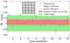 |
Fig. 4 Curvature radius as a function of lenses position. Each point corresponds to the average of the measurements on 4 different optical matrices, and the error bars represent the standard deviation between these 4 measurements. The uncertainty of measurement is ± 30 μm. Each lens is identified by a number (lens position). A mark (where the PMMA was injected during molding) ensures the same lens identification on all four matrices. The red dashed lines represent the tolerance analysis calculated in Section 2.3. The green area corresponds to the ranges of R that meet the fixed constraints (even if the tolerance is not met), while the red area indicates the data ranges where resistive losses reach 13% (>10% set), as explained at the end of Section 2.3. |
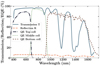 |
Fig. 5 Transmission (T) and reflection (R) of PMMA. EQE of each sub-cell is also plot, the data comes from the wafer supplier datasheet [15]. |
4 Electrical and optical modeling
A model was constructed to estimate the micro-CPV prototype short-circuit current. This model can be used to isolate and evaluate the system various optical losses. The model is based on radiometric equations mainly on the calculation of the spectral irradiance incident on the solar cell, denoted Einc(λ), as shown in Equation (2):
 (2)
(2)
where Esource is the AM1.5D solar spectrum, RPMMA(λ) and RPDMS(λ) are the reflection coefficients at the Air-PMMA and PMMA-PDMS interfaces, TPMMA(λ) and TPDMS(λ) are the transmittances of the PMMA and PDMS layers.
For Equation (2), several parameters are required, such as reflection and transmission for PMMA and PDMS. Reflection and transmission measurements of PMMA (RPMMA and TPMMA) have been carried out and are shown in Figure 5 in Section 3. The transmission values for the PDMS (TPDMS) used in this study (sylgard 184) have been found in the literature [16]. Reflection at the PMMA/PDMS (RPDMS) interface was calculated using the optical index.
From Equation (2), the current in the cell and each sub-cell can be calculated using the EQE presented in Figure 5. The presented EQE in Figure 5 is obtained for an interface with glass. In our case, the interface is with PDMS. Since the refractive index are similar, we will assume that the reflections at the interface are identical.
Figure 6 shows the optical transmission for each interface and material that light has to pass through before reaching the cell. The highest optical losses are due to the PDMS absorption for the top cell and the PMMA absorption for the bottom cell. PMMA absorption losses at top cell and middle cell wavelengths are low. At the cell scale, optical losses of the concentrating module are predominantly present in the bottom cell spectrum.
The output current of each sub-cell based on the model at a DNI of 1000 W/m2 at 350×, with and without losses due to concentrating optics, has been calculated in order to see the optical losses impact on the monomodule performance. The results are shown in Figure 6. Whether losses are considered or not, the top cell has the minimal output current. Therefore, the top cell stays the limiting sub-cell. The greatest current loss occurs in the bottom sub-cell. Since this sub-cell has excess current, it does not generate any electrical loss. These losses can even be advantageous, as they limit cell overheating due to excess current by approaching a current matching configuration, even though some of the heat absorbed by the PMMA still contributes to the warming of the cell.
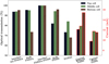 |
Fig. 6 Optical transmission for each interface/material for each sub-cell. These calculations were performed for the top cell between 400 nm and 700 nm, for the middle cell between 700 nm and 900 nm, and for the bottom cell between 900 nm and 1700 nm. The output current of each sub-cell at a DNI of 1000 W/m2 at 350×, with and without losses due to concentrating optics (reflection/absorption and metallization), corresponds to the two values on the right in red. |
5 Micro-CPV module fabrication
In this section, the aim is to build a prototype module. The manufacture of the cells, their connection and the alignment of the optics will be discussed in this part.
5.1 Cells fabrication
A commercial wafer with InGaP/InGaAs/Ge triple-junctions epitaxy has been used for the manufacture of micro solar cells with an area of 0.25 mm2 used in this study. Front contact is made by evaporation of Pd/Ge/Ti/Pd/Al (50/100/50/50/1000 nm) [17]. This metallization limits the cells series resistance, thereby improving performance at high concentrations. The cells are then electrically isolated by plasma etching (SiCl4/Cl2/H2) [18]. This type of plasma produces sidewalls with few defects, thus reducing perimeter recombination losses [19]. The addition of hydrogen to the plasma also enables passivation of the sidewalls, again reducing perimeter recombination [18]. The rear contact is made by evaporation over the entire surface of Ni/Au (50/1000 nm) [18]. An enhanced chemical vapor deposition (PECVD) deposit of SiN/SiO (66/69 nm) is then deposited on the front face and opened by CF4 plasma etching to expose contact regions [19]. This layer acts as an anti-reflective coating. Solar cells are then singulated ('diced') by plasma etching using a Bosch process [20]. This cutting method is used because it reduces the width of trenches compared with Saw-Dicing, thus saving materials when manufacturing micro-cells [21]. The wafer used to fabricate these cells is not optimized for concentration, so the cells will be used here as sensors to evaluate the optical performances of the system.
5.2 Connection of cells
In this section, cell connection method is presented. It is made on a silicon substrate where the two contacts (front and rear) are transferred. Electrical insulation of the substrate is ensured with a 50 nm deposition of SiO2. The surface is then metallized by evaporation of Ti/Cu (500/1000 nm) to create the pads where the cells are soldered. A tin-silver-copper (Sn-Ag-Cu or SAC) paste is then screen-printed onto Ti/Cu pads and cells are placed on pads using a pick-and-place equipment. A reflow process is then performed at 270 °C to melt the solder. This solder not only provides the electrical connection to the rear face of the cell, but also acts as a heat sink. Moreover, the effects of capillarity during soldering will also help to recenter the cell, allowing alignment precision of the order of a few microns [22]. With the cells now soldered and aligned on the silicon substrate, a drop of epoxy (EPO-TEK 301-2) is deposited next to the cell. The drop wets the substrate and the edges of the cell, creating a slight slope which connects the front face of the cell and the substrate [23]. The electrical connection between the front pad and the substrate is then made with a silver paste deposited on the epoxy.
During the metallization of the substrate, alignment marks (10 μm wide) are also deposited to help with the next step of alignment of the optics.
5.3 Optics alignment
The aim of this section is now to align and bond the PMMA optics to the Silicon substrate to which the cells are connected. The first step is to place spacers that ensure a 1.5 mm gap between the top of the cells and the PMMA optics, to reach the PDMS thickness used in the simulations (see Sect. 2.2). Positioning is carried out so that each spacer is in the angle of the PMMA optic, which will help with alignment. Once this stage has been completed, the Newport SOL1A solar simulator fitted with a Keithley 2601 EMS is used to check the current. The optic is positioned over the receiver using an optical microscope to achieve a first alignment between optic in PMMA and alignment marks on the receiver. The alignment is then adjusted to maximise the current. Aligning with 10 μm wide marks, in addition to checking the current to obtain the maximum enable us to readily respect the 115 μm tolerance computed in Section 2.1. Once the alignment is complete, the optic is adhesively attached to the receiver at the spacers. Once the adhesive has dried, PDMS (Sylgard 184) is poured between the receiver and the PMMA optic and cured at room temperature.
5.4 Final prototype
Figure 7 shows a picture of the final prototype. The cells can be seen through the edge of the PMMA block, indicating a good quality of interface between PMMA and PDMS. Once the prototype is completed, the PDMS thickness can be measured. As with PMMA, a caliper is used to measure the entire module from which the thickness of the PMMA optics and silicon wafer (≈200 μm with the thickness of the weld) must be removed. The measured thickness of the PDMS is finally 1.48 mm. PDMS thickness is therefore well controlled and in line with the tolerances presented in Section 2.3 (1.5 ± 0.305 mm).
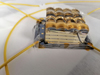 |
Fig. 7 Picture of the final prototype. |
6 Measurements of optical performance
6.1 Outdoor characterization
The outdoor characterization of the micro-CPV module was carried out in the solar park of the Institut Interdisciplinaire d'Innovation Technologique (3IT) of the Université de Sherbrooke using an EKO-Keithley 2-axis tracker. This tracker allows to follow the sun on two axes (azimuth and elevation) with a precision of ±0.01°. A Raspberry pi microcomputer is used to drive the EKO tracker and a Keithley 2601B source measurement unit to measure electrical characteristics of each individual solar cell. Two solar cells have been measured, one positioned under lens number 2 (cell A) and the other under lens number 13 (cell B), corresponding to lenses with a curvature radius close to that simulated (see Fig. 4).
The first step of outdoors measurement is to make a current map of 900 points as a function of azimuth and elevation. This map has two purposes, (1) To find the point of maximum current corresponding to optimal sun/lens/cell alignment to add an offset to the tracking to correct potential mechanical misalignment. (2) To measure the module acceptance angle. The measured current was normalized by Direct Normal Irradiance (DNI [W/m2]). The azimuth and elevation values were converted into angle of incidence using the point of greatest current as a reference, assuming normal incidence at the position corresponding to the maximum normalized short-circuit current. Since we are considering monomodules, the short circuit current based acceptance angle is supposed to be equal to the maximum power based acceptance angle [24]. The normalized current as a function of angle of incidence is plotted in Figure 8. The black dotted line is the threshold corresponding to 90% of the maximum normalized current. On the curve, several values of angle of incidence correspond to the 90% threshold. This can be explained by the fact that the metallization on the cell is not symmetrical, as can be seen in Figure 8. The shading percentage will vary depending on the direction in which the light spot moves, which will impact the generated current. Considering the upper limit of the curve, which corresponds to the case where the light shifts towards the area without busbars (towards right on the picture Fig. 8), we find an acceptance angle of 0.5°, as predicted by ZEMAX simulations done in Section 2.3. On the other hand, if the light is shifted towards the busbar (towards left on the picture Fig. 8), which corresponds to the lower limit of the curve, then the acceptance angle will be 0.25° (this angle has also been checked in ZEMAX simulations, considering metallization). The average acceptance angle is 0.38°, which is slightly below the IEC 62670 standard, which sets the minimum acceptance angle at ±0.4°. Our acceptance angle can easily be improved by reducing the size of the busbar [23].
After determining the acceptance angle of the module, the objective is to measure the short-circuit current as a function of the DNI received by the cell to compare the result with model presented in Section 4 and study the optical efficiency of the module.
The module was left for several hours on May 10, 2024. The data was then filtered using the ASTM E2527 method described in IEC 62670-3 to plot the short-circuit current as a function of the DNI received by the module. It imposes restrictions on data regression, including an ambient temperature range between 10 °C and 30 °C, direct irradiance greater than 750 W/m2, diffuse irradiance less than 140 W/m2, and data rejection in the event of DNI deviation greater than 2% over 10 min [25]. As the measurements were carried out on a particularly cloudy day (between 150 and 350 W/m2 of diffuse irradiance), the diffuse irradiance condition was removed (the measured currents are therefore slightly overestimated).
Figure 9 shows the short circuit current (Isc) as a function of the DNI. Blue and orange scatter plots represent the outdoor measurements for each cell, the blue and orange continuous curves correspond to the linear fit (Pearson correlation coefficient of 0.93 and 0.94 for A and B respectively) of the measured data. The green curve corresponds to the modeled data described in Section 4. Since the DNI directly impacts the delivered current, the data in Figure 6 has been extended over a wider range of DNI to compare it with outdoor measurements.
The model predicts current quite accurately. Indeed, an average deviation of only 2.6% with cell A and 4.1% with cell B can be observed. This small difference can be explained by shading. Metallization is taken into account in the model on the basis of the top cell illumination, as shown in Figure 2, which corresponds to a shading loss of 6.7%. If the curvature radius is greater than 6.83 mm, then the size of the light spot on the top cell will be reduced, which reduces shading losses. Moreover, the diffuse irradiance is not taken into account in the model. The current is therefore slightly overestimated. Taking a diffuse irradiance of 350 W/m2 and an incidence angle of 0.5°, an increase in the incident power of 0.26% can be estimated (see Appendix A.4).
The measured current and the model are very close, which means that there is no significant loss of light on the cell. Therefore, all the parameters of the optical system are well controlled and there are few form errors in the lenses, particularly for the conicity constant, which could not be verified in Section 3.
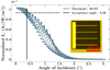 |
Fig. 8 Normalized Isc of cell A as a function of the rays incidence angle and a picture of the front face of cells. |
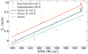 |
Fig. 9 Isc depending on DNI for 2 micro solar cells and modeled data. |
6.2 Optical efficiency
Now the model has been validated according to the outdoor measurements, we used it to assess the optical efficiency of our system. Since we are working with monomodules, we cannot directly refer to CTM (Cell-to-Module) losses, as there are no current mismatch losses that could range from 1% to 5% [26]. We are therefore talking about optical efficiency here.
From current calculated in Figure 6 validated by measurement, the optical efficiency can be calculated:
 (3)
(3)
In the literature, CTMs for micro-CPV modules range from 71.4% to 86.7% [26]. Taking into account the current mismatch losses, our module is in agreement with the literature and the CTM could easily be increased by replacing the PDMS (sylgard 184) to a less absorbent PDMS or another material. By halving the losses related to the top cell level, the optical efficiency could exceed 90%.
7 Conclusion
A compact optical system for micro-CPV has been designed, manufactured and characterized. The simulations and models match up well with the measurements. An optical efficiency of 81% has been calculated and experimentally validated, and it could easily be increased by changing the PDMS layer which absorbs a lot for the top cell wavelengths (18.09% absorbed) which are limiting the current. PMMA absorbs strongly at bottom cell wavelengths (24.61% absorbed) but the top cell remains limiting. Finally, we have shown that it is possible to produce a high-performance and low-cost optical system. Future work could improve the precision of the optics molding, particularly in terms of curvature radius. New measurements should also be made with less diffuse irradiance, and by changing the PDMS used in this article to a less absorbent material.
Acknowledgments
LN2 is a joint international Research Laboratory (IRL 3463) funded and co-operated in Canada by Université de Sherbrooke (UDS) and in France by CNRS as well as ECL, INSA Lyon, and Université Grenoble Alpes (UGA). We acknowledge the support from NSERC (Canada), Prompt (Quebec) and STACE through the MARS-CPV project. The support from Yanis Prunier for in-field measurements and for acceptance angle calculation is acknowledged.
Funding
This research was fund by CRSNG and Prompt through Mars-CPV project.
Conflicts of interest
The authors have nothing to disclose.
Data availability statement
Data will be made available on request.
Author contribution statement
Writing − Original Draft Preparation: Corentin Jouanneau, Marius Denain. Writing − Review & Editing: All authors. Visualization: Corentin Jouanneau, Thomas Bidaud. Methodology: Corentin Jouanneau, Konan Kouame, Maxime Weiss, Jean-Francois Bryche, Artur Turala. Formal analysis: Corentin Jouanneau, Thomas Bidaud, Marius Denain. Conceptualization: Corentin Jouanneau, Thomas Bidaud, Léo Guernion. Data Curation: Corentin Jouanneau, Marius Denain, Thomas Bidaud. Supervision: Gwenaëlle Hamon, Maxime Darnon, Thomas Bidaud, David Danovitch. Funding acquisition: Gwenaëlle Hamon, Maxime Darnon.
References
- Best Research-Cell Efficiency Chart. https://www.nrel.gov/pv/cell-efficiency.html (visited on 06/06/2024) [Google Scholar]
- A. Richter, M. Hermle, S.W. Glunz, Reassessment of the limiting efficiency for crystalline silicon solar cells, IEEE J. Photovolt. 3, 1184 (2013), https://doi.org/10.1109/JPHOTOV.2013.2270351 [CrossRef] [Google Scholar]
- N. Jost, T. Gu, J. Hu, C. Domínguez, I. Antón, Integrated micro-scale concentrating photovoltaics: a scalable path toward high-efficiency, low-cost solar power, Sol. RRL 7, 2300363 (2023), https://doi.org/10.1002/solr.202300363 [CrossRef] [Google Scholar]
- G.M. Wilson, M. Al-Jassim, W.K. Metzger, S.W. Glunz, P. Verlinden, G. Xiong, L.M. Mansfield, B.J. Stanbery, K. Zhu, Y. Yan, J.J. Berry, A.J. Ptak, F. Dimroth, B.M. Kayes, A.C. Tamboli, R. Peibst, K. Catchpole, M.O. Reese, C.S. Klinga, P. Denholm, M. Morjaria, M.G. Deceglie, J.M. Freeman, M.A. Mikofski, D.C. Jordan, G. TamizhMani, D.B. Sulas-Kern, The 2020 photovoltaic technologies roadmap, J. Phys. D: Appl. Phys. 53, 493001 (2020), https://doi.org/10.1088/1361-6463/ab9c6a [CrossRef] [Google Scholar]
- M. Steiner, A. Bösch, A. Dilger, F. Dimroth, T. Dörsam, M. Muller, T. Hornung, G. Siefer, M. Wiesenfarth, A.W. Bett, FLATCON® CPV module with 36.7% efficiency equipped with four-junction solar cells, Prog. Photovolt.: Res. Appl. 23, 1323 (2015), https://doi.org/10.1002/pip.2568 [CrossRef] [Google Scholar]
- H. Arase, A. Matsushita, A. Itou, T. Asano, N. Hayashi, D. Inoue, R. Futakuchi, K. Inoue, T. Nakagawa, M. Yamamoto, E. Fujii, Y. Anda, H. Ishida, T. Ueda, O. Fidaner, M. Wiemer, D. Ueda, A novel thin concentrator photovoltaic with microsolar cells directly attached to a lens array, IEEE J. Photovolt. 4, 709 (2014), https://doi.org/10.1109/JPHOTOV.2013.2292364 [CrossRef] [Google Scholar]
- R. Norman, E. Leveille, N. Caillou, J. Blais, S. Rosa, V. Aimez, L.G. Frechette, Molding arrays of tertiary optical elements for microcell receivers, AIP Conf. Proc. 2550, 040006 (2022), https://doi.org/10.1063/5.0099160 [CrossRef] [Google Scholar]
- K.A.W. Horowitz, D.W. Cunningham, J. Zahler, An analysis of techno-economic requirements for MOSAIC CPV systems to achieve cost competitiveness, in Light, Energy and the Environment (Optica Publishing Group, 2017), paper RM3C.4. https://doi.org/10.1364/OSE.2017.RM3C.4 [Google Scholar]
- B. Furman, E. Menard, A. Gray, M. Meitl, S. Bonafede, D. Kneeburg, K. Ghosal, R. Bukovnik, W. Wagner, J. Gabriel, S. Seel, S. Burroughs, A high concentration photovoltaic module utilizing micro-transfer printing and surface mount technology, in 2010 35th IEEE Photovoltaic Specialists Conference. (2010), p. 000475, https://doi.org/10.1109/PVSC.2010.5616766 [Google Scholar]
- N. Hayashi, A. Matsushita, D. Inoue, M. Matsumoto, T. Nagata, H. Higuchi, Y. Aya, T. Nakagawa, Nonuniformity sunlight-irradiation effect on photovoltaic performance of concentrating photovoltaic using microsolar cells without secondary optics, IEEE J. Photovolt. 6, 350 (2016), https://doi.org/10.1109/JPHOTOV.2015.2491598 [CrossRef] [Google Scholar]
- O. Fidaner, F.A. Suarez, M. Wiemer, V.A. Sabnis, T. Asano, A. Itou, D. Inoue, N. Hayashi, H. Arase, A. Matsushita, T. Nakagawa, High efficiency micro solar cells integrated with lens array, Appl. Phys. Lett. 104, 103902 (2014), https://doi.org/10.1063/1.4868116 [CrossRef] [Google Scholar]
- A. Itou, T. Asano, D. Inoue, H. Arase, A. Matsushita, N. Hayashi, R. Futakuchi, K. Inoue, M. Yamamoto, E. Fujii, T. Nakagawa, Y. Anda, H. Ishida, T. Ueda, O. Fidaner, M. Wiemer, D. Ueda, High-efficiency thin and compact concentrator photovoltaics using micro-solar cells with via-holes sandwiched between thin lens-array and circuit board, Jpn. J. Appl. Phys. 53, 04ER01 (2014), https://doi.org/10.7567/JJAP.53.04ER01 [CrossRef] [Google Scholar]
- N. Hayashi, D. Inoue, M. Matsumoto, A. Matsushita, H. Higuchi, Y. Aya, T. Nakagawa, High-efficiency thin and compact concentrator photovoltaics with micro-solar cells directly attached to a lens array, Opt. Express 23, A594 (2015), https://doi.org/10.1364/OE.23.00A594 [Google Scholar]
- N. Jost, G. Vallerotto, A. Tripoli, S. Askins, C. Domínguez, I. Antón, Demonstration of molded glass primary optics for high-efficiency micro-concentrator photovoltaics, Sol. Energy Mater. Sol. Cells 245, 111882 (2022), https://doi.org/10.1016/j.solmat.2022.111882 [CrossRef] [Google Scholar]
- CPV Solar Cells − AZUR SPACE Solar Power GmbH. https://www.azurspace.com/index.php/en/products/products-cpv/cpv-solar-cells (visited on 06/21/2024) [Google Scholar]
- V. Prajzler, M. Neruda, M. Květoň, Flexible multimode optical elastomer waveguides, J. Mater. Sci.: Mater. Electr. 30, 16983 (2019), https://doi.org/10.1007/s10854-019-02087-1 [CrossRef] [Google Scholar]
- P. Huo, I. Rey-Stolle, Al-based front contacts for HCPV solar cell, AIP Conf. Proc. 1881, 040004 (2017), https://doi.org/10.1063/1.5001426 [CrossRef] [Google Scholar]
- M. de Lafontaine, E. Pargon, C. Petit-Etienne, G. Gay, A. Jaouad, M-J. Gour, M. Volatier, S. Fafard, V. Aimez, M. Darnon, Influence of plasma process on III-V/Ge multijunction solar cell via etching, Sol. Energy Mater. Sol. Cells 195, 49 (2019), https://doi.org/10.1016/j.solmat.2019.01.048 [CrossRef] [Google Scholar]
- P. Albert, A. Jaouad, G. Hamon, M. Volatier, C.E. Valdivia, Y. Deshayes, K. Hinzer, L. Béchou, V. Aimez, M. Darnon, Miniaturization of InGaP/InGaAs/Ge solar cells for micro-concentrator photovoltaics, Prog. Photovolt.: Res. Appl. 29, 990 (2021), https://doi.org/10.1002/pip.3421 [CrossRef] [Google Scholar]
- M. Darnon, M. de Lafontaine, M. Volatier, S. Fafard, R. Arès, A. Jaouad, V. Aimez, Deep germanium etching using time multiplexed plasma etching, J. Vac. Sci. Technol. B 33, 060605 (2015), https://doi.org/10.1116/1.4936112 [CrossRef] [Google Scholar]
- M. Darnon, M. de Lafontaine, P. Albert, C. Jouanneau, T. Bidaud, C. Dubuc, M. Volatier, V. Aimez, A. Jaouad, G. Hamon, Sub-millimeter-scale multijunction solar cells for concentrator photovoltaics (CPV), in Proc. SPIE 11996, Physics, Simulation, and Photonic Engineering of Photovoltaic Devices XI. (2022), Vol. 11996, p. 49. https://doi.org/10.1117/12.2613441 [Google Scholar]
- V. Vareilles, E. Kaiser, P. Voarino, M. Wiesenfarth, R. Cariou, F. Dimroth, M. Veschetti, Y. Amara, H. Helmers, Experimental and simulative correlations of the influence of solder volume and receptor size on the capillary self-alignment of micro solar cells, J. Microelectromech. Syst. 33, 290 (2024), https://doi.org/10.1109/JMEMS.2024.3352396 [CrossRef] [Google Scholar]
- C. Jouanneau, T. Bidaud, A. Turala, D. Danovitch, G. Hamon, M. Darnon, A novel parallel interconnection approach to reduce shading losses on submillimeter concentrated photovoltaic technologies, in 2024 IEEE 74th Electronic Components and Technology Conference (ECTC). (2024), p. 2205, https://doi.org/10.1109/ECTC51529.2024.00375 [Google Scholar]
- K. Araki, H. Nagai, R. Herrero, I. Antón, G. Sala, K-H. Lee, M. Yamaguchi, 1-D and 2-D Monte Carlo simulations for analysis of CPV module characteristics including the acceptance angle impacted by assembly errors, Sol. Energy 147, 448 (2017), https://doi.org/10.1016/j.solener.2017. 03.060 [CrossRef] [Google Scholar]
- A.J. Kinfack Leoga, A. Ritou, M. Blanchard, L. Dirand, Y. Prunier, P. St-Pierre, D. Chuet, P-O. Provost, M. Volatier, V. Aimez, G. Hamon, A. Jaouad, C. Dubuc, M. Darnon, Outdoor characterization of solar cells with microstructured antireflective coating in a concentrator photovoltaic monomodule, IEEE J. Photovolt. 13, 736 (2023), https://doi.org/10.1109/JPHOTOV.2023.3295498 [CrossRef] [Google Scholar]
- A. Ritou, Développement, fabrication et caractérisation de modules photovoltaïques à concentration à ultra haut rendement à base de micro-concentrateurs, PhD thesis, Université Grenoble Alpes, 2018 [Google Scholar]
Cite this article as: Corentin Jouanneau, Marius Denain, Léo Guernion, Thomas Bidaud, Konan Kouame, Maxime Weiss, Artur Turala, David Danovitch, Jean-François Bryche, Maxime Darnon, Gwenaëlle Hamon, Design, manufacture and characterization of compact optics for micro-CPV, EPJ Photovoltaics 16, 27 (2025), https://doi.org/10.1051/epjpv/2025015
Appendix A
A.1 Calculation to define ϵ
Equation (A.1) describes the difference in the aberrant optical path associated with the crossing of a dioptre of radius R, conicity constant ϵ and an aperture h. The optical indexes before and after the dioptre are n and n':
 (A.1)
(A.1)
The optical conjugation of the dioptre is described by z and z', which are the position of the image before and after the dioptre. Qz is then defined as the longitudinal invariant defined by Equation (A.2)
 (A.2)
(A.2)
In order to cancelled spherical aberrations and therefore the n′Δ in Equation (A.1) the conicity constant is set to −0.46.
A.2 1D resistive model
Transfer Lenght Method (TLM) measurements have been performed on state of the art multi-junction solar cells based on a commercial epi-wafer to determine the contact resistivity (Rcont 6.2 × 10⁻⁶ ohm cm2) and the lateral resistivity (Rlat = 500 ohm square). Finally, the finger width has been fixed to be w = 4.4 μm, which is the conventional width obtained when performing evaporation and photolithography processes in our lab. For the sake of simplicity, we considered that a modification on the spot size induces only a variation in the light concentration. Then Cmean has been set constant equal the Cgeometric = 350× as it corresponds to the case where the light is perfectly transmitted through the optics and spread on the top surface. Based on these results and assumptions we fixed the different parameters (Rcont, Rlat and the fingers thickness) and optimized the spacing between the fingers for each concentration using a simple 1D model. All the losses (contact resistive losses Pcontact, lateral resistive losses Plateral, resistive losses in the finger Pfinger and shadowing losses Pshadow) have been summarized in the scheme displayed in Figure A.1.
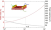 |
Fig. A.1 Estimation of resistive losses and shadowing power losses (red curve) as a function pf the PAR. The 10% power loss is marked by a red dashed line as a virtual guide. The finger spacing (dark curve) has been optimized for each concentration. The scheme presents all the losses (arrows) considered in the model: Power loss in the model (light green arrow), the power loss to the metal contact (dark green), the lateral resistance (black) and the shadowing (blue). |
A.3 Radius of curvature measurement
A Keyence − VK-X1100 confocal microscope was used. Measurements were taken at the top of the lenses with an X20 zoom. The 16 lenses of 4 different optics were measured. In order to remove the noise and refocus the measured data on the vertex, a quadratic fit was performed on all the measurements. This quadratic fit allows to find the top of the lens with greater precision. The radius of curvature can be then found using the equation for an aspheric lens (Eq. (A.3)).
 (A.3)
(A.3)
With:  with the point (0,0) found with the quadratic fit, Rc the curvature radius, ϵ the conicity constant.
Figure A.2 shows the profile of a measured lens (scatter plot in blue) and its associated aspheric fit (black curve) as a function of radius r. The fit matches with the scatter plot and the radius of curvature can therefore be determined using this method. In the case of the lens shown in Figure A.2, the curvature radius is 6.88 mm. The measurement uncertainty is 3σRc =0.03 mm.
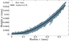 |
Fig. A.2 Fit performed to find the radius of curvature. The curvature radius is 6.88mm. |
A.4 Impact of diffuse irradiance
Considering an acceptance angle of 0.5°, the percentage of sky available to concentrate diffuse light is  . Now considering a diffuse radiation power of 350 W/m2 and a concentration of 350× on a 0.25 mm2 cell, the incident diffuse power is 0.003 × 350 × 350 × 2.5 × 10−7. To this, we can add the diffuse radiation passing through the sides of the lenses: 2.5 × 10−7*350. The total diffuse power reaching the cell is therefore: 1.8 × 10⁻⁴. Comparing this value to the power reaching the cell with a DNI of 800 W/m2 (350×2.5×10−7×800), the percentage of diffuse light is therefore: 0.26%.
All Tables
Summary of the concentration optics parameters as well as its alignment tolerances and the specifications studied here.
All Figures
|
Fig. 1 Optical system diagram. The PMMA lenses are 19.9 mm-thick from the top of lenses. |
| In the text | |
|
Fig. 2 ZEMAX optical simulation of the illuminance of a 0.25 mm2 solar cell as a function of wavelength A) 500 nm (top cell), B) 800 nm (middle cell) and C) 1300nm (bottom cell). The scale on the right of the images corresponds to the effective concentration. The average concentration is 350×, so from the maximum effective concentration of each sub-cell, we can calculate the PAR for each sub-cell: top cell: 2.38, middle cell: 6.85, bottom cell: 15.6. |
| In the text | |
|
Fig. 3 Picture of a PMMA matrix lenses after molding. |
| In the text | |
|
Fig. 4 Curvature radius as a function of lenses position. Each point corresponds to the average of the measurements on 4 different optical matrices, and the error bars represent the standard deviation between these 4 measurements. The uncertainty of measurement is ± 30 μm. Each lens is identified by a number (lens position). A mark (where the PMMA was injected during molding) ensures the same lens identification on all four matrices. The red dashed lines represent the tolerance analysis calculated in Section 2.3. The green area corresponds to the ranges of R that meet the fixed constraints (even if the tolerance is not met), while the red area indicates the data ranges where resistive losses reach 13% (>10% set), as explained at the end of Section 2.3. |
| In the text | |
|
Fig. 5 Transmission (T) and reflection (R) of PMMA. EQE of each sub-cell is also plot, the data comes from the wafer supplier datasheet [15]. |
| In the text | |
|
Fig. 6 Optical transmission for each interface/material for each sub-cell. These calculations were performed for the top cell between 400 nm and 700 nm, for the middle cell between 700 nm and 900 nm, and for the bottom cell between 900 nm and 1700 nm. The output current of each sub-cell at a DNI of 1000 W/m2 at 350×, with and without losses due to concentrating optics (reflection/absorption and metallization), corresponds to the two values on the right in red. |
| In the text | |
|
Fig. 7 Picture of the final prototype. |
| In the text | |
|
Fig. 8 Normalized Isc of cell A as a function of the rays incidence angle and a picture of the front face of cells. |
| In the text | |
|
Fig. 9 Isc depending on DNI for 2 micro solar cells and modeled data. |
| In the text | |
|
Fig. A.1 Estimation of resistive losses and shadowing power losses (red curve) as a function pf the PAR. The 10% power loss is marked by a red dashed line as a virtual guide. The finger spacing (dark curve) has been optimized for each concentration. The scheme presents all the losses (arrows) considered in the model: Power loss in the model (light green arrow), the power loss to the metal contact (dark green), the lateral resistance (black) and the shadowing (blue). |
| In the text | |
|
Fig. A.2 Fit performed to find the radius of curvature. The curvature radius is 6.88mm. |
| In the text | |
Current usage metrics show cumulative count of Article Views (full-text article views including HTML views, PDF and ePub downloads, according to the available data) and Abstracts Views on Vision4Press platform.
Data correspond to usage on the plateform after 2015. The current usage metrics is available 48-96 hours after online publication and is updated daily on week days.
Initial download of the metrics may take a while.