| Issue |
EPJ Photovolt.
Volume 16, 2025
|
|
|---|---|---|
| Article Number | 28 | |
| Number of page(s) | 8 | |
| DOI | https://doi.org/10.1051/epjpv/2025016 | |
| Published online | 08 October 2025 | |
https://doi.org/10.1051/epjpv/2025016
Original Article
Towards crack free fabrication of interconnect shingled solar modules through wire length and wire-end geometry control
Institute for Solar Energy Research Hamelin (ISFH), Am Ohrberg 1, Emmerthal, 31860, Germany
* e-mail: This email address is being protected from spambots. You need JavaScript enabled to view it.
Received:
21
March
2025
Accepted:
24
August
2025
Published online: 8 October 2025
Abstract
Reduction or elimination of cell-to-cell distance in a solar panel is a straightforward way to enhance solar module efficiency. Overlapping interconnection by wire shingling increases the active area in solar modules and allows to apply mainstream stringer technology, which reduces the cost of integration. However, since commonly used wires for interconnection have diameter of about 300 μm, mechanical load during lamination can result in crack formation. In this work, we demonstrate the potential for adapting process parameters and cell-wire configurations to eliminate crack formation in wire shingling technology. Our crack formation analysis identifies three types of crack formations that occur during the lamination of half-cut cells. These are cross cracks located close to the wire ends, v-shaped cracks at the overlap wire feedthrough in rear as well as in front cell. With short wire length and elliptical wire-end-shape, along with conventional lamination parameters and non-alternating cell arrangement we take the first successful step towards a feasible solution for the crack-free fabrication of shingled wire interconnect solar modules.
Key words: Interconnect shingling / interconnection wires / shingle plate / M6 PERC cells
© C. Xu et al., Published by EDP Sciences, 2025
 This is an Open Access article distributed under the terms of the Creative Commons Attribution License (https://creativecommons.org/licenses/by/4.0), which permits unrestricted use, distribution, and reproduction in any medium, provided the original work is properly cited.
1 Introduction
Among other techniques, reduction or elimination of cell-to-cell distance in a solar panel is a straightforward way to improve solar module efficiency by effectively raising the proportion of active area for photocurrent harvesting, a method that is seeing increasing application [1]. Based on the interconnect technologies, the main technologies for this idea include shingling of cut cells by electric conductive adhesives (ECA) [2–13], interconnect shingling of halved cells with ribbons [14] and interconnect shingling with round wires [15,16] as well as shingling with both ECA and ribbons [17]. Each idea faces different challenges during production for various cell technologies, lamination materials and cell arrangement. For interconnect shingling of halved cells, wires or ribbons could intensify the local mechanical load on the laser-groove edge, resulting in more cracks in halved cells [18]. One possible mitigation of such problem is applying geometry modification of interconnection wires like tiling ribbons [19]. For ECA shingled modules, the reduction of silver consumption is in the focus of the present research, for example by decreasing the ECA amount [20] or replacing expensive Ag with other conductive materials like intrinsically conductive adhesive (ICA) [21]. However, as the fingers need to carry the current over the full cell width, e.g. one sixth of the wafer length, instead of only the path to the next interconnect, e.g. 1/24 in case of a 12-busbar cell due to symmetric collection of current by the busbars. This requires significantly larger amounts of Ag paste for current cell technologies and is not compatible with fine line printing resulting in current and resistive losses. The crack formation at the joint between ECA and solar cell through temperature cycling suggests careful material selection and process optimization for shingled cells with adhesive [22]. Moreover, the interconnection-induced resistance in ECA shingled modules has to be optimized as well [10,12]. The cell-to-module (CTM) ratio of efficiency is 96% and of power 97% for the ribbon shingling [14], higher than the non-passivated ECA shingling [23]. An effective way to reduce the recombination loss at the defect sites on the halved cell edges in ECA shingles modules is to carry out edge passivation, which adds 0.5% relative to the pseudo fill factor by and a power boost of about 1% with respect to the non-passivated shingled modules [10], while for ECA shingling without passivation the CTM of power is 95.5% [23]. For the other technologies like interconnect-shingling of halved cells with ribbons [14] and interconnect shingling with wires [15,16], the mechanical load builds up considerably as the cells overlap with each other, which raises concern about field performance even after a crack-free production. The impact of these cracks on power loss seems to be low, however it is still a phenomenon found in the field and could be avoided [24]. In this paper, we investigate the use of half M6 PERC bifacial cells with a thickness of 165 µm with 380 µm diameter wires as interconnects to explore cell crack formation and potential solutions for cell crack prevention. Both the cell edge and the wire geometries are found to play a significant role in crack formation. By modifying wire geometry and cell arrangement, crack-free modules can be produced.
2 Material and methods
Full PERC M6 mono crystalline silicon cells with pseudo square corners and a length of 166 mm are laser scribed from rear side and mechanically cleaved (LSC) by bowing the cell. With laser spot of 20 µm radius, laser energy density for LSC process is around 21.65 J/cm2. After LSC, each half cell has 9 busbars, where there are 6 rectangular soldering pads on front side and 3 soldering pads on rear side along each busbar. The corresponding busbar pitches on front side and on rear side are 13.5 mm and 27 mm, respectively. Scanning electron microscopy reveals, that the edge without laser groove (green arrow in Fig. 1) shows no defects due to the saw damage etching carried out during cell processing, whereas the laser-groove-edge (red arrow in Fig. 1) has a high concentration of surface defects. Therefore, the edge without laser groove is expected to be mechanically more stable than the laser groove edge. Taking a detailed look on the laser groove edge, the laser groove side (red rectangles with rounded corners in Fig. 1) has more defects than the broken edge side (yellow rectangles with rounded corners in Fig. 1).
After LSC step, the interconnect wires are soldered to the rear side of each cell, which is also the laser groove side (Fig. 2a). The soldered cell-wire units are then placed on an aluminum shingle plate with cell front side up and the wires from the rear side are soldered onto the front side of the next cell, which is repeated till the whole string is complete (Fig. 2b). The aluminum shingle plate with a total thickness of around 2 mm has two steps as stop edges with step height of around 0.6 mm, where the step length is 82 mm for a fixed 1 mm cell overlap in a cell string. The half cells are soldered in a string with 9 wires of 380 μm diameter on the heated Al shingle plate with a surface temperature of 105°C ± 3°C to precisely control the overlap length. The wires are round copper with a yield strength of 100 N/mm2, coated with SnPb 60/40 solder alloy (melting point 183–190 °C). Fixed with brass blocks, the wires are soldered directly onto the busbars using a 5 mm-wide soldering tip at 260–280 °C, with positioning tolerance of about 100 µm. Although Figures 2a and 2b show a non-alternating cell arrangement, an alternating arrangement can be achieved by rotating the upper cell in Figure 2b by 180° and feeding its wires through the laser groove edge instead of edge without laser groove. At the end the soldered cell string has the cell rear side up and the 3 mm thick low-iron tempered glass front layer, 450 μm polyolefine encapsulant foil, cell string, 450 μm polyolefine encapsulant foil and 280 μm thick white backsheets are stacked up in the laminator. With the controlled temperature and pressure, lamination is performed (Fig. 2c) in a laboratory laminator from Stange GmbH, with a total process time of around 21 min. The maximum pressures and temperatures for different laminates are listed in Table 1, while the ramping steps and cooling step are depicted in Figure 4. We apply a 0.45 mm polyolefin elastomer (POE) encapsulant foil as interlayer between glass and cells, and between cells and backsheets. Electroluminescence (EL) is employed for characterizing the cracks formed during lamination. The POE was chosen for its high transmittance − over 40% in the UV range between 250 nm and 400 nm in the cured state after heating to 150 °C, whereas traditional encapsulants like ethylene vinyl acetate (EVA) have a UV-cutoff at 375 nm in the cured state [25].
Table 1 shows all prepared string configurations. We test the influence of various factors, including the cell arrangement (the orientation and location of cell edges with laser-groove), the wire length (whether the wire extends to the end of the solder pad as short or to the cell edge as long), the wire shape (whether the wire is curved or straightened), the wire end shape (whether the wire is round or flattened at the wire end), the maximum set pressure during the lamination procedure and the maximum set lamination temperature. Unrolled and separated from the roles, each interconnection wire naturally curves even without any mechanical load. However, this curvature might introduce stress during the soldering process. We straighten the wires before soldering by pulling them over a defined curved edge, making soldering easier. To reduce mechanical stress in the solar cells, the wire ends are flattened. For this, each wire is fixed onto a metal surface using double-sided tape. A metal block, positioned upright like a hinge and named as hinge-block, is then lowered onto a spacer block to define the pressing angle. A mechanical force is applied with a hammer upon the hinge-block with 1.5 cm thickness. By adjusting the spacer height, the flattened length is controlled between 2 mm and 8 mm, with 3 mm yielding the best results with ∼0.9 mm maximum local width. Since the copper-wire is thin and ductile in comparison to the hinge-block, it conforms to the shape defined by the design geometry and is not particularly sensitive to variations in the applied hammer force. The photo for the optimized wire end prior to soldering process is presented in the inset of Figure 2a. The length of the wire is controlled by adjusting the feeding length at the cutting machine. It has to be mentioned that depending on the cell arrangement, the wires are either in contact with the edge without laser groove and the broken edge side for the non-alternating cell arrangement as in Figure 2b, or the wires are in contact with two edges without laser groove for the alternating cell arrangement (Fig. 3a, green rectangular), or the wires are in contact with the laser groove edge and the broken edge side by the alternating cell arrangement (Fig. 3a, blue rectangular). Therefore, the cell arrangement plays an important role in the cell crack result.
To investigate the impact of the difference between edge with and without laser groove, we fabricate 3-cell-laminates with alternating cell arrangements (sample O1 and O2 in Tab. 1). To study the crack formation process, we fabricate another 3-cell-laminate (sample P1 in Tab. 1) with a non-alternating cell arrangement. The lamination process is intentionally stopped at different stages, varying pressure and temperature values as listed in Table 1. After each step, we remove the sample, let it cool, and perform EL imaging. After EL imaging the sample is placed again in the laminator to carry out the process till next datapoint. Additionally, we fabricate six samples (G1 to G6 in Tab. 1) to analyze the influence of wire geometry on crack formation, using EL measurements for assessment.
The IU characterization of the crack-free laminate is carried out on a halm Moduletest 3 sun simulator with a xenon lamp. Measurement temperatures are kept at 25 °C and the pulse duration for the measurement in this work is 93 ms. One pulse is utilized for each cycle containing forward and backward IV-sweeps, which are performed during illumination, collecting 500 data points per sweep with a time interval of 0.018 ms per data point. For a complete forward-backward cycle a total of 1000 data points per curve pair are collected. The EL measurement is carried out in the integrated EL tool in the halm Moduletest3 sun simulator with 5 A and 5.2 V, with an exposure time of 0.5 s.
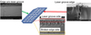 |
Fig. 1 Illustration of the edges with (red arrow) and without (green arrow) laser groove. The top left SEM image shows a wafer edge without laser groove. The top right SEM image perpendicular to the laser pattern shows a slice through the laser groove on the rear side of the cell prior to mechanical cleaving. The bottom SEM image parallel to the laser pattern displays the edge after cleaving. The upper part, which was scribed by the laser (marked red), has a rough surface (rear side of the solar cell), while the lower part, the cleaved edge, appears similarly smooth compared to the original edge on the other side of the cell. |
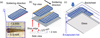 |
Fig. 2 (a) Illustration of the soldering process on the rear side of one solar cell. The rear side is the laser groove side. (b) Illustration of the soldering process with an aluminum shingle form (grey) with two steps acting as stop edges (red arrows) to control the shingling distance for the manual stringing process. For clarity both the top view and the side view of the shingle plate are supplied. (c) Illustration of the lamination process with the stack structure with encapsulant foil, backsheet and the glass. The thick arrow indicates the direction of the pressure during lamination process. |
Overview of samples and module tests. In “Cell arrangement” column, each “<” or “>” represents a solar cell, with the arrow pointing towards the edge without laser groove. For example, the conventional arrangement for 3 half‑cells in a string is “<<<”. Wirelength “Short” refers to the interconnect wires reaching to the last solder pad, while wirelength “Long” refers to interconnect wires reaching close to the cell edge.
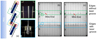 |
Fig. 3 (a) The cell arrangement with two edges without laser groove (marked green) overlapping each other (cell 1 and 2)and with laser groove edges (marked blue) overlapping each other (cell 2 and 3). (b) and (c) are the EL images of two 3-cell-laminates containing both cell arrangement in (a) with the overlapping region marked with corresponding colors. |
3 Results
3.1 Influence of edges on the crack formation
Here we focus the results on the cell cracks at the cell overlap in sample O1 and O2. In Figure 3a, the laser groove side (marked red) of lower cell is toward wires. Figures 3b and 3c correspond to the sample O1 and O2 in Table 1, respectively. String in Figure 3b is with interconnect wires reaching to the last solder pad named as short wire, where the distance between solder pad and cell edge is 8.22 ± 0.41 mm, while the string in Figure 3c is with interconnect wires reaching close to the cell edge named as short wire, see red arrow. Two images of the wire between the two cells (green frame in Fig. 3b) and the end of wire at the last soldering pad (blue frame in Fig. 3b) are presented as well, with arrows indicating their locations. All the cells are tabbed on both sides, while the overlap length is kept as 1 mm for all overlapping cells. We observe a trend of more cracks with laser groove edge overlapping, which is correlated to the defective rich laser groove edge (blue frames in Figs. 3c and 3d). A detailed observation in Figure 3c is, along the laser groove edge in the cell 3 cracks are identified, while the other laser groove edge in cell 2 in the middle cell shows no crack.
In the next we discuss about the possible physical mechanism behind the crack formation in the cells. The microcracks exist most on the laser groove side due to laser scribing process and significantly reduces the fracture stress [26]. During the lamination process, photovoltaic cells are positioned atop interconnect wires. As lamination pressure increases, the cells are mechanically deformed around the wire geometry, inducing tensile stress across the rear surfaces of the cells. This tensile loading promotes the initiation and propagation of microcracks, particularly on the cell's rear side. Compared to the front surface, microcracks in the rear are more susceptible to evolving into critical fractures due to the higher tensile strain concentration in that region during lamination. Therefore, if two laser groove edges are overlapping each other with interconnection wires lying in between, the laser groove rear side with tensile strain is showing more cracks.
Close to edge without laser groove, cracks are observed as well, see green blue frames in Figures 3c and 3d. By varying the wire length, we verified that these cracks locate exactly at the wire ends. Moreover, by the edge without laser groove with short interconnect wires (green frame in Fig. 3c), much smaller cracks are identified than with the long interconnect wires (green frame in Fig. 3d). The crack-ratio with short interconnect wires is 2/9, while the crack-ratio with long interconnect wires is 5/9.
This observation indicates the strong impact of the cell interconnect wire on the crack formation process, while the maximum lamination pressure and temperature are pivotal as well. In the following sections, we will show these two important factors with respect to their interplay.
3.2 Analysis of the crack formation
To better analyze the crack formation process, we intentionally stop the lamination at different stages, at varying pressure and temperature values as listed in Table 1 for sample P1. After each step, we remove the sample, let it cool, and perform EL imaging. We repeat this process multiple times. The set temperature and pressure during these processes are plotted as scatters in Figures 4a and 4b, respectively. The lamination process is interrupted at the marked points. These data points, at which the EL images are taken, are noted with the corresponding letters. The dashed lines with arrows indicate the process flow for one exemplary process to take EL images shown in Figure 5d. All the cells are tabbed on both sides, while the overlap length is kept as 1 mm for all overlapping cells.
The stopping temperatures and pressures are listed above each EL image in Figures 5a–5f. The max. set lamination temperature is 155 °C and the max. set pressure is 1 × 10⁵ Pa. The circles mark the cracks appeared at 155 °C and 9 × 10⁴ Pa as well as 155 °C and 1 × 10⁵ Pa. By setting broken edge side to face the glass, three half-cells are shingled together with 1 mm overlap with non-alternating order. We observe the first crack formation after 155°C and 9 × 10⁴ Pa are reached (Fig. 5e). Between 9 × 10⁴ Pa and 1 × 10⁵ Pa at 155°C most of the cracks form at the end of the interconnection wires (Fig. 5f). Therefore, for the further study the maximum pressure is set to 7 × 10⁴ Pa and 8 × 10⁴ Pa to avoid crack formation.
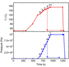 |
Fig. 4 The temperature a) and pressure b) profiles for the lamination of interconnect singled strings. |
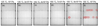 |
Fig. 5 (a) to (f) are the EL images of the 3-cell-laminates taken out at various interruption points with the noted interruption temperature and pressure in Figure 4. |
3.3 Influence of the interconnect wire geometry
We fabricate six samples (G1 to G6 in Tab. 1) to analyze the influence of wire geometry on crack formation, using EL measurements for assessment. To analyze the impact of the wire end to the crack formation we show the results of 3 influencing factors of the wire separation process. First a non-perfect wire cut can lead to wire curvature at the wire end. The influence of non-perfect and straight wire cut ends are compared. Second, the influence of flattening (elliptic form) of the wire at the wire end is compared to non-flattened wire ends (round form). Third, the influence of wires reaching up to the end of the final solder pad and up to the end of the cell edge. For the evaluation process we count each wire transit region between two wafers as one possible origin of cell cracks. Take the longest string G5 as an example, as we have 10 cells with 9 wires and 9 wire transit regions between two wafers (overlap of cells) we have 81 regions with possible origin of cell cracks. In the following these regions are called wire-cell contact. All results are show in a compact form in Figure 4.
We observe that the wire geometry has a strong impact on the crack-ratio at the wire-cell contacts. An optimized cell arrangement is chosen as illustrated in Figure 6a. The dashed frames indicate three different positions: at wire ends (green), on the broken edge side of the front cell (blue), and near the edge without a laser groove edge in the rear cell (purple). The distinction between front cell and rear cell is referred to the wire-cell contact, i.e. the front cell contacts the wire from front, while the rear cell contacts the wire from rear. This description corresponds to the observation through the glass and aligns with EL image. With broken edge side to the glass and non-alternating arrangement, the crack formation due to defective laser groove edge should be minimized. We conclude three main types of cracks among various laminates in the EL image captures from glass side: first, the cross cracks in the front cell located close to the wire end (Type 1, in the green frame in Fig. 6b); second, the V-shaped cracks at the overlap wire feedthrough in rear cell (Type 2, in the purple frame in Fig. 6b); third, the V-shaped cracks at overlap wire feedthrough in front cell (Type 3, in the blue frames in Fig. 6b). The cross cracks (Type 1) are depicted by a crack initiation stress point on the surface of the cell, whereas the V-shape cracks (Type 2 and 3) are characterized by crack initiation stress points on the edge of rear or front cells. The cracks geometric forms and their appearance positions are both different. Since the wire geometry includes curvature, length and wire end form, we adjust these three parameters separately and illustrate the influence of each factor in Figure 7. For each bar in the plot in Figure 7, the number of wire-cell contacts is 18*(n−1), where n is the total number of cells that is listed in Table 1. For samples from G1 to G6, the total numbers of wire-cell contacts are 36, 36, 36, 36, 162, 108, respectively. Since different total numbers of wire-cell contacts are investigated, we define the crack-free-ratio as the ratio of crack-free wire-cell contacts to the total number of contacts, whereas the crack-ratio as the ratio of wire-cell contacts with cracks to the total number of contacts. First, by changing the wire end form from round to elliptic (compare samples G1 and G2 in Tab. 1), one can expect an increased crack-free-ratio from 93% to 95 % by reducing cracks Type 3 at 155 °C and 8 × 10⁴ Pa. However, this change is not significant and not sufficient for 100% crack-free wire-cell contact. Second, by changing the wire from curved to straight with round wire end form (compare samples G3 and G4 in Tab. 1), the Type 1 cracks vanish for lamination condition of 150°C and 7 × 10⁴ Pa but not for 8 × 10⁴ Pa. Finally, by reducing the wire length to not long than the last solder pad by keeping wire straight and with elliptic wire end form (compare samples G5 and G6 in Tab. 1), the Type 2 cracks can be eliminated at 155 °C and 8 × 10⁴ Pa.
With the optimized wire geometry and the optimized process, we fabricated a module with 7 cells and 1 mm cell overlap (G6 in Tab. 1). In this 7-cell laminate module, no cell cracks are observed by the electroluminescence image (Fig. 8). The IU characteristics (Fig. 9) as well as the important electrical parameters (Tab. 2) from 3 forward and backward voltage sweeps show a well performing solar module. While the process validation is still ongoing, further confirmation of the optimized fabrication process is planned using a large batch of solar modules produced with automated manufacturing.
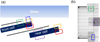 |
Fig. 6 (a) The cell arrangement with broken edge facing the glass. (b) Here EL images of the three described crack types (Type 1, 2, and 3 with green, purple and blue frames, respectively). |
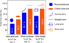 |
Fig. 7 Bar plot for the crack-free-ratio with different interconnect wire geometries. The corresponding ratio values are supplied at each bar. |
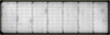 |
Fig. 8 The EL image of the laminated 7-cell module shows an intact, crack-free structure. |
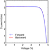 |
Fig. 9 The current voltage characteristics of the laminated 7-cell module shows a well performing solar module. |
Important electrical parameters extracted from the 3 times forward and backward current-voltage measurements on the 7-cell module presented in Figure 8. ISC is the short circuit current, UOC is the open circuit voltage, PMPP is the maximum power, η is the aperture efficiency of the module, FF is the fill factor.
4 Conclusions
We present a detailed analysis of how the interconnect wire geometry affects crack formation during the lamination of half-cut PERC cells with interconnect shingling. These findings are helpful for further developing industrial production of densely packed PV modules with interconnect shingling.
Our crack formation analysis identifies three types of crack formations that occur during the lamination of M6 PERC half-cut cells: (1) cross cracks located close to the wire ends, (2) v-shaped cracks at the overlap wire feedthrough in rear cell as well as (3) v-shaped cracks at overlap wire feedthrough in front cell. With less curvature, short wire length and elliptical wire-end-shape, along with conventional lamination parameters and non-alternating cell arrangement we do not observe crack in the laminated module. This could supply a feasible solution for high throughput industrial fabrication of wire interconnect solar modules. Since in the production of solar modules the nominal procedure comprises stretching, the curvature of wire is guaranteed low. The wire length and wire-end-shape could contribute to control parameters that are crucial for crack formation. The short wires further reduce the consumption of silver containing wires, which is already silver saving by avoiding using ECA.
As revealed by our previous study in our group [23], we noticed that the total thickness of the lamination stack including cell and wire strongly changes the mechanical load. As ITRPV report in 2024 pointed out [1], the silicon heterojunction (SHJ) and tunneling oxide passivated contacts (TOPCon) solar cells are around 10–20 μm thinner than the rest types of solar cells, the mechanical load in modules with SHJ and TOPCon solar cells should be lower than the modules with other cell technology. A further reduction of crack-ratio is expected by the similar process presented in this paper.
The impacts from other aspects, like the encapsulant foil thickness, wire thickness and backsheet mechanical properties are not discussed in this study but should be taken into account in further investigations of the lamination process. Thorough investigation on root cause for crack formation in shingling with ECA has been carried out by Klasen et al. [22], where the scanning electron microscopy (SEM) reveals the microstructure along the crack formation and the finite element modeling (FEM) suggests the complete picture of strain and stress situation. In the future, the detailed analysis as for shingling with ECA could be carried out to study these interesting points.
Among others, the technology for reducing cell edge defects can also help reducing crack formation. In comparison to the technology of cell separation in this work LSC, the cells can also be sliced into half-cells using thermal laser separation (TLS). By using this technology, the amount of cell edge defects, which are main reason for the crack formation, can be significantly reduced [5,27].
During the highly automatic fabrication process, the wire geometry can be controlled by the stringer machine. The wire length can be adjusted by the cutting step and positioning of solar cells. The wire end geometry requires an extra step of pressing, but could be achievable. The wire shape is in most cases well regulated, since the wires are spanned prior to being fed to the surface of cells by the wire feeding unit in the stringer machines. Therefore, we expect realization of the optimization of these three geometric features.
Acknowledgments
The authors would like to thank Susanne Blankemeyer for fruitful discussion. The authors would like to thank the halm elektronik GmbH for supplying the flasher with integrated electroluminescence and corresponding technical support.
Funding
This research was funded by the state of Lower Saxony and the Federal Ministry for Economic Affairs and Energy (BMWE) under grant number 03EE1004 (ProVe).
Conflicts of interest
The authors have nothing to disclose.
Data availability statement
Data associated with this article are available from the corresponding author, C. Xu, upon reasonable request.
Author contribution statement
Conceptualization, C. Xu, H. Schulte-Huxel and M. Köntges; Methodology, C. Xu and B. Wolpensinger; Validation, I. Kunze and B. Wolpensinger; Formal Analysis, C. Xu; Investigation, B. Wolpensinger.; Resources, M. Köntges; Writing − Original Draft Preparation, C. Xu; Writing − Review & Editing, Schulte-Huxel and M. Köntges; Visualization, C. Xu; Supervision, C. Xu; Project Administration, C. Xu; Funding Acquisition, M. Köntges.
References
- ITRPV, Photovoltaics equipment international technology roadmap for photovoltaics (ITRPV) 2023 results (2023) [Google Scholar]
- N. Wöhrle, E. Lohmüller, M. Mittag, A. Moldovan, P. Baliozian, T. Fellmeth et al., Solar cell demand for bifacial and singulated-cell module architectures, Photovolt. Int. 36, 48 (2017) [Google Scholar]
- P. Baliozian, E. Lohmüller, T. Fellmeth, N. Wöhrle, A. Krieg, R. Preu, Bifacial p-type silicon shingle solar cells − the “pSPEER” concept, Sol. RRL 2, 1700171 (2018) [Google Scholar]
- M. Al-Akash, P. Baliozian, E. Lohmüller, T. Fellmeth, N. Wöhrle, R. Preu, Metallization Fraction Of Bifacial pSPEER Shingle Solar Cells, in 35th European PV Solar Energy Conference and Exhibition (Brussels, Belgium, 2018), pp. 564–568 [Google Scholar]
- P. Baliozian, E. Lohmüller, T. Fellmeth, N. Wöhrle, A. Krieg, R. Preu, Bifacial shingle solar cells on p-type Cz-Si (pSPEER), AIP Conf. Proc. 1999, 110002-1 (2018) [CrossRef] [Google Scholar]
- W. Oh, J. Park, S. Dimitrijev, E.K. Kim, Y.S. Park, J. Lee, Metallization of crystalline silicon solar cells for shingled photovoltaic module application, Sol. Energy 195, 527 (2020) [Google Scholar]
- D. Rudolph, J. Rabanal-Arabach, I. Ullmann, A. Halm, A. Schneider, T. Fischer, Cell design optimization for shingled modules, in 33rd European Photovoltaic Sol. Energy Conference and Exhibition (2017), pp. 880–883 [Google Scholar]
- N. Klasen, A. Mondon, A. Kraft, U. Eitner, Shingled cell interconnection: a new generation of bifacial PV-modules, in 7th Workshop on Metallization and Interconnection for Crystalline Silicon Solar Cells (April 15, 2018) [Google Scholar]
- J.D. Huyeng, E. Lohmüller, B. Shabanzadeh, C. Reichel, T. Rößler, J. Weber et al., Challenges and advantages of cut solar cells for shingling and half-cell modules, EPJ Photovolt. 15, 22 (2024) [Google Scholar]
- J. Weber, L. Kniffki, L. Gutmann, J. Huyeng, E. Lohmüller, T. Rößler, Investigating the impact of edge passivation on shingle solar modules, Sol. Energy Mater. Sol. Cells 271, 112876 (2024) [Google Scholar]
- J. Weber, T. Rößler, Electrically conductive adhesive-free interconnection of shingle solar cells, Sol. Energy Mater. Sol. Cells 261, 112517 (2023). Available from: https://www.sciencedirect.com/science/article/pii/S0927024823003380 [Google Scholar]
- J. Weber, T. Roessler, How to assess the electrical quality of solar cell interconnection in shingle solar modules, Prog. Photovolt.: Res. Appl. 31, 949 (2023) [Google Scholar]
- M. Kronsbein, L. Böck, K. Dyhr, T. Rößler, N. Willenbacher, Less is more: Enabling low-filled electrically conductive adhesives for shingled solar cell interconnection using the capillary suspension concept, Sol. Energy Mater. Sol. Cells 287, 113603 (2025) [Google Scholar]
- H. Schulte-Huxel, S. Blankemeyer, A. Morlier, R. Brendel, M. Köntges, Interconnect-shingling: maximizing the active module area with conventional module processes, Sol. Energy Mater. Sol. Cells 200, 109991 (2019). Available from: https://www.sciencedirect.com/science/article/pii/S0927024819303204 [CrossRef] [Google Scholar]
- A. Faes García, M. Despeisse, J. Levrat, J. Champliaud, N. Badel, M. Kiaee, T. Söderström, Y. Yao, R. Grischke, M. Gragert, J. Ufheil, P. Papet, B. Strahm, B. Cattaneo, J. Cattin, Y. Baumgartner, A. Hessler-Wyser, C. Ballif Reyes LE, A. Faes, M. Despeisse, J. Levrat, J. Champliaud, N. Badel et al., Smartwire solar cell interconnection technology, in PVSEC 29th (2014), pp. 2555–2561 [Google Scholar]
- P. Papet, S. Hänni, L. Andreetta, T. Kossler, D. Lachenal, B. Legradic et al., Overlap modules: a unique cell layup using smart wire connection technology, AIP Conf. Proc. 2147, 080001 (2019) [Google Scholar]
- L. Theunissen, B. Willems, J. Burke, D. Tonini, M. Galiazzo, A. Henckens, Electrically conductive adhesives as cell interconnection material in shingled module technology, AIP Conf. Proc. 1999, 080003 (2018) [Google Scholar]
- S. Hwang, Y. Kang, Reliability study on the half-cutting PERC solar cell and module, Energy Rep. 10, 678 (2023) [Google Scholar]
- W.S. Tao, G.C. Bao, J.H. Liu, M. Zhang, L.C. Wang, J. Dai, Y.Y. Huang, Y. Du, Z. Zhang, H. Jin, Modeling and experimental investigations of thermo-mechanical stress induced micro-cracks in different crystalline silicon photovoltaic modules, SSRN Electron. J. (2022). Available at: https://ssrn.com/abstract=4046698 [Google Scholar]
- C. Kaiser, V. Nikitina, T. Geipel, A. Kraft, Reduction of ECA amount for the ribbon interconnection of heterojuction solar cells, in 37th European Photovoltaic Solar Energy Conference and Exhibition (2020), pp. 1086–1090 [Google Scholar]
- A.X. Chen, N.A. Azpiroz, S.E. Brew, A.M. Valdez, G.L. Esparza, Y. Qie et al., Silver-free intrinsically conductive adhesives for shingled solar cells, Cell Rep. Phys. Sci. 5, 101967 (2024) [Google Scholar]
- N. Klasen, F. Heinz, A. De Rose, T. Roessler, A. Kraft, M. Kamlah, Root cause analysis of solar cell cracks at shingle joints, Sol. Energy Mater. Sol. Cells. 238, 111590 (2022) [Google Scholar]
- D. Von Kutzleben, T. Rößler, M. Mittag, J. Weber, S. Sigdel, N. Klasen et al., Development of shingle matrix technology for integrated Pv applications, in 8th World Conference on Photovoltaic Energy Conversion (Milan, Italy, 26-30 Septembrer 2022), pp. 26–30 [Google Scholar]
- M. Köntges, J. Lin, A.V.G.C. Eder, G. Oreski, P. Hacke, J.S. Stei et al., Degradation and failure modes in new photovol- taic cell and module technologies, Report IEA-PVPS (2025) [Google Scholar]
- G. Oreski, A. Omazic, G.C. Eder, Y. Voronko, L. Neumaier, W. Mühleisen et al., Properties and degradation behaviour of polyolefin encapsulants for photovoltaic modules, Prog. Photovolt.: Res. Appl. 28, 1277 (2020) [Google Scholar]
- S. Eiternick, F. Kaule, H.U. Zühlke, T. Kießling, M. Grimm, S. Schoenfelder et al., High quality half-cell processing using thermal laser separation, Energy Procedia 77, 340 (2015) [Google Scholar]
- A. Muenzer, P. Baliozian, K. Ahmed, A. Nair, E. Lohmüller, T. Fellmeth, A. Spribille RP, Laser assisted separation processes for bifacial pSPEER shingle solar cells, in 37th European Photovoltaic Solar Energy Conference and Exhibition (2020), pp. 394–399 [Google Scholar]
Cite this article as: Chencheng Xu, Bettina Wolpensinger, Iris Kunze, Henning Schulte-Huxel, Marc Köntges, Towards crack free fabrication of interconnect shingled solar modules through wire length and wire-end geometry control, EPJ Photovoltaics. 16, 28 (2025), https://doi.org/10.1051/epjpv/2025016
All Tables
Overview of samples and module tests. In “Cell arrangement” column, each “<” or “>” represents a solar cell, with the arrow pointing towards the edge without laser groove. For example, the conventional arrangement for 3 half‑cells in a string is “<<<”. Wirelength “Short” refers to the interconnect wires reaching to the last solder pad, while wirelength “Long” refers to interconnect wires reaching close to the cell edge.
Important electrical parameters extracted from the 3 times forward and backward current-voltage measurements on the 7-cell module presented in Figure 8. ISC is the short circuit current, UOC is the open circuit voltage, PMPP is the maximum power, η is the aperture efficiency of the module, FF is the fill factor.
All Figures
|
Fig. 1 Illustration of the edges with (red arrow) and without (green arrow) laser groove. The top left SEM image shows a wafer edge without laser groove. The top right SEM image perpendicular to the laser pattern shows a slice through the laser groove on the rear side of the cell prior to mechanical cleaving. The bottom SEM image parallel to the laser pattern displays the edge after cleaving. The upper part, which was scribed by the laser (marked red), has a rough surface (rear side of the solar cell), while the lower part, the cleaved edge, appears similarly smooth compared to the original edge on the other side of the cell. |
| In the text | |
|
Fig. 2 (a) Illustration of the soldering process on the rear side of one solar cell. The rear side is the laser groove side. (b) Illustration of the soldering process with an aluminum shingle form (grey) with two steps acting as stop edges (red arrows) to control the shingling distance for the manual stringing process. For clarity both the top view and the side view of the shingle plate are supplied. (c) Illustration of the lamination process with the stack structure with encapsulant foil, backsheet and the glass. The thick arrow indicates the direction of the pressure during lamination process. |
| In the text | |
|
Fig. 3 (a) The cell arrangement with two edges without laser groove (marked green) overlapping each other (cell 1 and 2)and with laser groove edges (marked blue) overlapping each other (cell 2 and 3). (b) and (c) are the EL images of two 3-cell-laminates containing both cell arrangement in (a) with the overlapping region marked with corresponding colors. |
| In the text | |
|
Fig. 4 The temperature a) and pressure b) profiles for the lamination of interconnect singled strings. |
| In the text | |
|
Fig. 5 (a) to (f) are the EL images of the 3-cell-laminates taken out at various interruption points with the noted interruption temperature and pressure in Figure 4. |
| In the text | |
|
Fig. 6 (a) The cell arrangement with broken edge facing the glass. (b) Here EL images of the three described crack types (Type 1, 2, and 3 with green, purple and blue frames, respectively). |
| In the text | |
|
Fig. 7 Bar plot for the crack-free-ratio with different interconnect wire geometries. The corresponding ratio values are supplied at each bar. |
| In the text | |
|
Fig. 8 The EL image of the laminated 7-cell module shows an intact, crack-free structure. |
| In the text | |
|
Fig. 9 The current voltage characteristics of the laminated 7-cell module shows a well performing solar module. |
| In the text | |
Current usage metrics show cumulative count of Article Views (full-text article views including HTML views, PDF and ePub downloads, according to the available data) and Abstracts Views on Vision4Press platform.
Data correspond to usage on the plateform after 2015. The current usage metrics is available 48-96 hours after online publication and is updated daily on week days.
Initial download of the metrics may take a while.