Fig. 2
Download original image
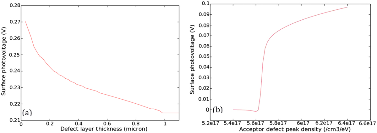
Surface photovoltage simulated (785 nm illumination 1000 W/m2) on bulk silicon doped n-type at ND = 1017 cm–3 (a) as a function of the thickness of the surface defect layer showing a reduction to a constant value for thick charge neutral layer and (b) as a function of acceptor defect density NDA (for defective layer thickness 0.1 μm) showing an initial reduction in SPV noted as a slight reduction in effective n-type doping, before NDA significantly larger than ND leads to the formation of an effective pn junction.
Current usage metrics show cumulative count of Article Views (full-text article views including HTML views, PDF and ePub downloads, according to the available data) and Abstracts Views on Vision4Press platform.
Data correspond to usage on the plateform after 2015. The current usage metrics is available 48-96 hours after online publication and is updated daily on week days.
Initial download of the metrics may take a while.