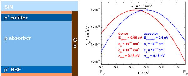
Fig. 1

Download original image
Left: Structural model of the poly-Si solar cell unit composed of a p-type crystalline Si absorber grain ( width), p+ back surface field and n+ emitter with an adjacent vertical grain boundary layer ( width). The contacts, defined as ohmic, are depicted in orange. The silicon nitride (SiN) top layer represents the antireflection coating. Right: Assumed defect distribution in the GB layer over the energy in the band gap for the particular case of a GB defect density of . For details see Tables 1 and 2.
Current usage metrics show cumulative count of Article Views (full-text article views including HTML views, PDF and ePub downloads, according to the available data) and Abstracts Views on Vision4Press platform.
Data correspond to usage on the plateform after 2015. The current usage metrics is available 48-96 hours after online publication and is updated daily on week days.
Initial download of the metrics may take a while.


