| Issue |
EPJ Photovolt.
Volume 3, 2012
|
|
|---|---|---|
| Article Number | 30302 | |
| Number of page(s) | 4 | |
| Section | Semiconductor Thin Films | |
| DOI | https://doi.org/10.1051/epjpv/2012011 | |
| Published online | 17 September 2012 | |
https://doi.org/10.1051/epjpv/2012011
Zn(O, S) layers for chalcoyprite solar cells sputtered from a single target
1
Helmholtz-Zentrum Berlin für Materialien und
Energie, Hahn-Meitner-Platz
1, 14109
Berlin,
Germany
2
Bosch Solar CISTech, Münstersche Str. 24, 14772
Brandenburg an der Havel,
Germany
a e-mail: This email address is being protected from spambots. You need JavaScript enabled to view it.
Received:
30
April
2012
Accepted:
19
July
2012
Published online:
17
September
2012
Abstract
A simplified Cu(In, Ga)(S, Se)2/Zn(O, S)/ZnO:Al stack for chalcopyrite thin-film solar cells is proposed. In this stack the Zn(O, S) layer combines the roles of the traditional CdS buffer and undoped ZnO layers. It will be shown that Zn(O, S) films can be sputtered in argon atmosphere from a single mixed target without substrate heating. The photovoltaic performance of the simplified stack matches that of the conventional approach. Replacing the ZnO target with a ZnO/ZnS target may therefore be sufficient to omit the CdS buffer layer and avoid the associated complexity, safety and recycling issues, and to lower production cost.
© Owned by the authors, published by EDP Sciences, 2012
 This is an Open Access article distributed under the terms of the Creative Commons Attribution-Noncommercial License 3.0, which permits unrestricted use, distribution, and reproduction in any noncommercial medium, provided the original work is properly cited.
1 Introduction
Zn(O, S) is emerging as one of the most promising materials to replace CdS in the buffer layer of chalcopyrite-based thin-film solar cells [1]. Successful preparation technologies include chemical bath deposition and atomic layer deposition. Sputtering, already established in mass production for other layers of the cell, may be another attractive deposition technology. Chalcopyrite cells and modules are prepared with an undoped sputtered ZnO layer (i-ZnO) on top of the CdS. Therefore, we may consider a sputtered Zn(O, S) layer a modification of the standard ZnO layer, eliminating the need for a dedicated buffer layer. Reasonable cell performance for this approach has been reported previously. The Zn(O, S) was prepared by co-sputtering from ZnO and ZnS targets [2] or by reactive sputtering from a ZnS target in an Ar/O2 gas mixture [3]. These methods are well suited for fundamental investigations because the S/(O + S) ratio can be freely adjusted for an optimal conduction band alignment. On the other hand, in order to develop a true drop-in replacement for the standard ZnO process, a non-reactive process without substrate heating and using a single target is much more appropriate. In this contribution we report selected properties of thin Zn(O, S) films sputtered from single mixed targets and demonstrate their successful application in solar cells.
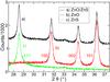 |
Fig. 1 XRD patterns of powder samples prepared from ZnO, ZnS and ZnO/ZnS sputtering targets. Miller indices are shown assuming hexagonal symmetry (wurtzite) for ZnO and cubic symmetry (zinc blende) for ZnS. |
2 Film preparation and properties
Targets with a nominal composition of S/(S + O) = 0.4 (atomic ratio) were procured from a commercial supplier. According to our energy dispersive X-ray spectroscopy (EDX) the ratio was 0.35. X-ray diffraction (XRD) patterns recorded with Cu Kα radiation (Fig. 1) revealed that the target material is a two phase mixture of ZnS and ZnO. Films were sputtered in pure Ar using 13.56 MHz (RF) plasma excitation in two different systems with target diameters of 75 (system A) and 125 mm (system B), respectively. The substrate was not moving during deposition. Typical parameters were working gas pressures in the range of 3−9 μbar and power densities of 1.3−1.7 W/cm2 which resulted in deposition rates of about 50 nm/min. The film composition was measured by EDX (film thickness ≈ 0.5 μm on glass/Mo substrates). The S/(S + O) ratio in the deposited films roughly reflected the composition of the target, however, it also depended on process parameters (Tab. 1). Films prepared at higher pressures were generally richer in sulphur. Similarly, substrate heating (if any) influences the sulphur content. We also found a radially symmetric inhomogeneity (Fig. 2) in the larger of the two deposition systems (system B without substrate heating). Furthermore, the sulphur content of the films increased slightly with target erosion. In contrast to our previous results with reactive sputtering, the sulphate (SO42−) and hydroxide contaminations as estimated from photo electron spectroscopy (XPS) were minimal even without deliberate substrate heating. XRD patterns of films (Fig. 3) sputtered onto heated substrates indicated a crystalline (wurtzite) structure with lattice constants approximately as expected from the S/(S + O) ratios. Without substrate heating, films did typically show only very weak XRD patterns. Optical transmission and reflection spectra (Fig. 4) were very similar to the ones measured for the reactively sputtered films, with the absorption being very low at longer wavelength and increasing rather slowly when approaching the band gap.
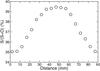 |
Fig. 2 S/(S + O) ratio across the substrate as measured by EDX. |
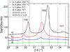 |
Fig. 3 XRD patterns of Zn(O, S) thin films on glass/Mo substrates prepared with and without substrate heating at two different Ar pressures. Vertical lines indicate calculated peak positions assuming hexagonal symmetry and a linear shift in lattice constants between ZnO and ZnS. |
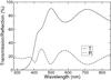 |
Fig. 4 Optical transmission (T) and reflection (R) of a Zn(O, S) film (thickness 400 nm) sputtered from a mixed target without substrate heating onto a soda lime float glass substrate. |
Composition of Zn(O, S) films as measured by EDX.
Parameters of the best cells (in-house total area measurements under simulated AM 1.5 illumination, without AR coating).
3 Device properties
Devices were prepared by using sequentially prepared glass/Mo/Cu(In, Ga)(S, Se)2 substrates from the Bosch Solar CISTech production line [4]. The full size substrates were cut into smaller pieces (2.5 × 2.5 or 5 × 5 cm2, depending on the sputtering system used) and sealed in dry atmosphere for shipping. Some samples were etched in aqueous KCN solution before depositing the Zn(O, S) layer. The thickness of the latter was in the range of 20 to 60 nm. Cells were completed with a sputtered ZnO :Al layer and Ni/Al grids evaporated through shadow masks. 32 cells with an area of 0.5 cm2 were defined on the 5 × 5 cm2 substrates by mechanical scribing. No anti-reflective coating was applied. Current-voltage (jV) characteristics were measured in-house with simulated AM 1.5 illumination without deliberate light soaking or post-annealing. The best efficiencies that could be achieved in a completely dry process (without etching) were reasonable but there was a distinct inhomogeneity across the substrate. Higher efficiencies, together with very good homogeneity, were achieved with the etched samples. Figure 5 shows a distribution of cell parameters measured on a 5 × 5 cm2 substrate. The performance in this case was comparable to reference cells prepared with the standard CdS/ZnO/ZnO :Al window on two 5 × 5 cm2 substrates cut from the same full size plate (absorbers not etched, only every other cell measured). Parameters of the best cells are given in Table 2. Considering these data, the new process results in better device performance than reactive sputtering [5]. The quantum efficiency (Fig. 6) shows better blue response for the cells with Zn(O, S)/ZnO :Al window. Using a tabulated AM 1.5 reference spectrum the calculated active area current densities are 37.1 mA/cm2 (CdS) and 38.1 mA/cm2, respectively, in good agreement with the total area short circuit current densities from jV measurements.
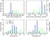 |
Fig. 5 Distribution of the parameters of small (0.5 cm2) cells with Zn(O, S)/ZnO :Al and CdS/ZnO/ZnO :Al windows on 5 × 5 cm2 substrates (see text) as measured under simulated AM 1.5 illumination. |
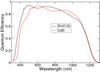 |
Fig. 6 Quantum efficiencies of CIGSSe/Zn(O, S)/ZnO :Al and CIGSSe/CdS/ZnO/ZnO :Al solar cells. |
4 Discussion
Due to the fact that the films did not always exhibit clear XRD patterns, it is difficult to unambiguously determine which phases are present in the films. Comparison of the optical band gap and cell parameters as a function of the overall S/(O + S) ratio with crystalline films prepared with substrate heating nevertheless suggest that the films are essentially compound ZnO1−xSx. Presumably, single phase Zn(O, S) films can be prepared by non reactive RF sputtering from a ZnO/ZnS mixed target without additional substrate heating. The optical band gap seems to be slightly higher than that of reactively sputtered films (with the same sulphur content) [6]. Lower sputtering pressure leads to slightly better crystallinity which may indicate that the growth is ion assisted. Inhomogeneity of the S/(O + S) ratio and drift of the latter with target erosion may be challenges in scaling-up of the process. Our previous studies conducted with varied S/(O + S) ratios (reactive sputtering) show a very rapid decline in fill factor and photo current density when there is too much sulphur in the Zn(O, S) film, presumably due to current blocking by a too high conduction band spike [6, 7]. The process is more tolerant on the oxygen-rich side of the optimum composition where the losses in open circuit voltage are not immediately critical. Compared to the previous results, the optimum sulphur content seems to be somewhat lower for the films sputtered from the mixed target (which may be connected to the different band gap mentioned above). In view of this, the composition of our targets was probably a little bit too sulphur rich. This is reflected in the cell results measured on as-grown substrates where the higher sulphur content beneath the center of the target already leads to partial current blocking and poor fill factor. It is interesting to note that etched absorbers appear to tolerate a higher S/(S + O) ratio. XPS shows (in agreement with literature data) that etching removes sodium containing compounds from the absorber surface. We may speculate that the presence of these sodium compounds induces a dipole at the absorber/Zn(O, S) interface which increases the tendency for too high a conduction band spike. The requirement for wet chemical surface conditioning is of course incompatible with the original goal of completely dry processing. However, we hope that a slightly more oxygen-rich target will remedy this problem. In any case, the device results reported here are clearly superior to the ones achieved previously by sputtering Cd-free materials directly onto a chalcopyrite absorber.
5 Summary and conclusions
RF sputtering from a ZnO/ZnS mixed target produces ZnO1−xSx films with different degrees of long range ordering. The S/(S + O) ratio in the film reflects the target composition but is also slightly influenced by process conditions. By transitioning from the previous approach (reactive sputtering onto heated substrates) to the one described here, we were able to almost close the efficiency gap between devices with sputtered Zn(O, S) layers and those with standard CdS/ZnO buffer. We have thus shown, that with a simple modification of the standard ZnO target, the Cd-containing buffer layer and its costly wet chemical preparation process may no longer be needed for efficient chalcopyrite solar cells.
Acknowledgments
We thank the Federal Ministry for the Environment, Nature Conservation and Nuclear Safety (BMU) for financial support of the NeuMaS project. Technical support in preparation and measurements by C. Kelch, M. Kirsch, C. Klimm, and L. Chikhaoui is gratefully acknowledged.
References
- N. Naghavi, D. Abou-Ras, N. Allsop, N. Barreau, S. Bücheler, A. Ennaoui, C.-H. Fischer, C. Guillen, D. Hariskos, J. Herrero, R. Klenk, K. Kushiya, D. Lincot, R. Menner, T. Nakada, C. Platzer-Björkman, S. Spiering, A.N. Tiwari, T. Törndahl, Prog. Photovolt. Res. Appl. 18, 411 (2010) [CrossRef] [Google Scholar]
- A. Okamoto, T. Minemoto, H. Takakura, Jpn J. Appl. Phys. 50, 04DP10 (2011) [CrossRef] [Google Scholar]
- A. Grimm, J. Just, D. Kieven, I. Lauermann, J. Palm, A. Neisser, T. Rissom, R. Klenk, Phys. Stat. Sol. RRL 4, 109 (2010) [CrossRef] [Google Scholar]
- V. Probst, F. Hergert, B. Walther, R. Thyen, G. Batereau-Neumann, B. Neumann, A. Windeck, T. Letzig, A. Gerlach, in Proceedings of the 24th European Photovoltaic Solar Energy Conference and Exhibition Munich, 2009, edited by W.C. Sinke, H.A. Ossenbrink, P. Helm (WIP, Munich, 2009), p. 2455 [Google Scholar]
- P. Pistor, A. Grimm, D. Kieven, F. Hergert, A. Jasenek, R. Klenk, in Proceedings of the 37th IEEE Photovoltaic Specialists Conference, Seattle, 2011 (IEEE, New York, 2011), p. 2812 [Google Scholar]
- A. Grimm, D. Kieven, R. Klenk, I. Lauermann, A. Neisser, T. Niesen, J. Palm, Thin Solid Films 520, 1330 (2011) [CrossRef] [Google Scholar]
- D. Kieven, A. Grimm, I. Lauermann, M.Ch. Lux-Steiner, J. Palm, T. Niesen, R. Klenk, Phys. Stat. Sol. RRL 6, 294 (2012) [CrossRef] [Google Scholar]
All Tables
Parameters of the best cells (in-house total area measurements under simulated AM 1.5 illumination, without AR coating).
All Figures
|
Fig. 1 XRD patterns of powder samples prepared from ZnO, ZnS and ZnO/ZnS sputtering targets. Miller indices are shown assuming hexagonal symmetry (wurtzite) for ZnO and cubic symmetry (zinc blende) for ZnS. |
| In the text | |
|
Fig. 2 S/(S + O) ratio across the substrate as measured by EDX. |
| In the text | |
|
Fig. 3 XRD patterns of Zn(O, S) thin films on glass/Mo substrates prepared with and without substrate heating at two different Ar pressures. Vertical lines indicate calculated peak positions assuming hexagonal symmetry and a linear shift in lattice constants between ZnO and ZnS. |
| In the text | |
|
Fig. 4 Optical transmission (T) and reflection (R) of a Zn(O, S) film (thickness 400 nm) sputtered from a mixed target without substrate heating onto a soda lime float glass substrate. |
| In the text | |
|
Fig. 5 Distribution of the parameters of small (0.5 cm2) cells with Zn(O, S)/ZnO :Al and CdS/ZnO/ZnO :Al windows on 5 × 5 cm2 substrates (see text) as measured under simulated AM 1.5 illumination. |
| In the text | |
|
Fig. 6 Quantum efficiencies of CIGSSe/Zn(O, S)/ZnO :Al and CIGSSe/CdS/ZnO/ZnO :Al solar cells. |
| In the text | |
Current usage metrics show cumulative count of Article Views (full-text article views including HTML views, PDF and ePub downloads, according to the available data) and Abstracts Views on Vision4Press platform.
Data correspond to usage on the plateform after 2015. The current usage metrics is available 48-96 hours after online publication and is updated daily on week days.
Initial download of the metrics may take a while.